Solutions
Question 1 Choose the correct option.
(i) In a BJT, largest current flow occurs
(A) in the emitter
(B) in the collector
(C) in the base
(D) through CB junction
(A) in the emitter
Reason : The emitter terminal, with its larger area compared to the collector and base terminals, experiences the largest current flow.
(ii) A series resistance is connected in the Zener diode circuit to
(A) Properly reverse bias the Zener
(B) Protect the Zener
(C) roperly forward bias the Zener
(D) Protect the load resistance
(B) Protect the Zener
Reason : To prevent the Zener diode from breaking during reverse biasing, a series resistance is added to protect it from exceeding its limit voltage.
(iii) A LED emits visible light when its
(A) junction is reverse biased
(B) depletion region widens
(C) holes and electrons recombine
(D) junction becomes hot
(C) holes and electrons recombine
Reason : Because on recombining of electrons and holes current flow occurs in PN junction diode and thus LED emits light.
(v) Solar cell operates on the principle of :
(A) diffusion
(B) recombination
(C) photo voltaic action
(D) carrier flow
(C) photo voltaic action
Reason : In photovoltaic action, generation of voltage takes place due to bombardment of the light photons.
(iv) A logic gate is an electronic circuit which:
(A) makes logical decisions
(B) allows electron flow only in one direction
(C) works using binary algebra
(D) alternates between 0 and 1 value
(A) makes logical decisions
Reason : A logic gate is an electronic circuit that makes logical decisions using various combinations of digital signals as inputs. It typically has one output but can accept multiple inputs. Connecting multiple logic gates allows for larger capabilities and combinational or sequential circuitry. A logic gate is an essential component of a digital circuit, with most having a single output and two inputs. Terminals are always in binary states, represented by a distinct voltage level.
Question 2 Answer in brief.
(i) Why is the base of a transistor made thin and is lightly doped?
The base of a transistor is lighter doped than the emitter and narrowed such that almost all electrons injected from the emitter (in a npn transistor) diffuse across the base to the collector junction without recombining with holes. That is, the base width is maintained less than the recombination distance. In addition, the emitter is significantly more highly doped than the base, resulting in higher emitter efficiency and common base current gain.
(ii) How is a Zener diode different than an ordinary diode?
A Zener diode is heavily doped, with doping concentrations greater than 1018 cm− 3 in both the p− and n− regions, whereas an ordinary diode has doping concentrations of 1017 cm− 3 or less. As a result, the peak inverse voltage (PIV) of an ordinary diode is
greater than that of a Zener diode, and the breakdown occurs through impact ionisation (avalanche process). Other than that, their I− V characteristics are similar.
(iii) On which factors does the wavelength of light emitted by a LED depend?
The intensity of the emitted light is directly proportional to the recombination rate and hence to the diode forward current.
The colour of the light emitted by an LED depends on the compound semiconductor material used and its composition (and doping levels) as given below :
LEDs are made with elements such as gallium, phosphorus and arsenic. By varying the proportions of these elements in the semiconducting materials, it is possible to produce light of different wavelengths.
- LED made using aluminium gallium arsenide (AlGaAs), it emits infrared radiations.
- LED made using gallium arsenic phosphide (GaAsP) produces either red or yellow light,
- LED made by using aluminium gallium phosphide (AlGaP) emits red or green light
- LED made by using zinc selenide (ZnSe) produce blue light.
(iv) Why should a photodiode be operated in reverse biased mode?
- A photodiode is operated in a reverse biased mode because as photodetector or photosensor, it must conduct only when radiation is incident on it.
- In the reverse biased mode, the dark current for zero illumination is negligibly small− of the order of few picoamperes to nanoamperes. But when illuminated, the photocurrent is several orders of magnitude greater.
(v) State the principle and uses of a solar Cell.
Principle : A solar cell works on the photovoltaic effect in which an emf is produced between the two layers of a pn− junction as a result of irradiation.
Use of Solar cell:
Solar cells used in domestic and space applications/
- A solar cell array, which consists of a collection of solar cells, is used during the day to power electrical equipment as well as to recharge batteries, which can then be utilised at night.
- Solar cell arrays supply electrical power to satellite equipment as well as isolated locations on Earth where electric power cables do not exist.
- Solar power generation systems on a large scale that are linked to the commercial power grid.
Question 3. Draw the circuit diagram of a half wave rectifier. Explain its working. What is the frequency of ripple in its output?
A device or a circuit which rectifies only one− half of each cycle of an alternating voltage is called a half− wave rectifier.
Electric circuit : The alternating voltage to be rectified is applied across the primary coil (PQ ) of a transformer. The secondary coil (AB) of the transformer is connected in series with the junction diode and a load resistance RL, as shown in below fig.
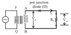
The alternating voltage across the secondary coil is the ac input voltage Vin. The dc voltage across the load resistance is called the output voltage Vout.
Working :
- Due to the alternating voltage Vin, the p− region of the diode becomes alternatively positive and negative with respect to the n− region.
- During the half− cycle when the p—region is positive, the diode is forward biased and conducts.
- A current IL passes through the load resistance RL in the direction shown.
- During the next half cycle, when the p− region is negative, the diode is reverse biased and the forward current drops to zero.
- Thus, the diode conducts only during one− half of the input cycle and thus acts as a half− wave rectifier.
- The intermittent output voltage Vout has a fixed polarity but changes periodically with time between zero and a maximum value. IL is unidirectional.
- Below figure shows the input and output voltage waveforms.
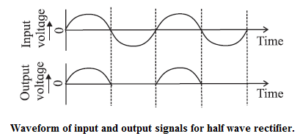
The pulsating dc output voltage of a half− wave rectifier has the same frequency as the input.
Question 4. Why do we need filters in a power supply?
- A rectifier's half− wave or full− wave output is a pulsing direct current that cannot be used directly in most electronic systems. These circuits require something closer to pure direct current, such as that supplied by batteries. A rectifier output, unlike a battery's pure dc waveform, contains an alternating current ripple on top of a dc waveform.
- A filter is a circuit that removes ripple from a direct current power source. A filter circuit can provide a highly smooth waveform that is similar to that produced by a battery. The most frequent filtering approach is to attach a capacitor across the rectifier's output.
Question 5. Draw a neat diagram of a full wave rectifier and explain it’s working.
Full Wave Rectifier:
A device or a circuit which rectifies both halves of each cycle of an alternating voltage is called a full− wave rectifier.
Electric circuit : The alternating voltage to be rectified is applied across the primary coil (PQ) of a transformer with a centre− tapped secondary coil (AB). The terminals A and B of the secondary are connected to the two p− regions of two junction diodes D1 and D2, respectively. The centre− tap C is connected to the ground. The load resistance RL is connected across the common n− regions and the ground.
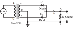
Working: During one half cycle of the input, terminal A of the secondary is positive while B is negative with respect to the ground (the centre− tap C). During this half cycle, diode D1 is forward biased and conducts, while diode D2 is reverse biased and does not conduct. The direction of current IL through RL is in the sense shown.
During the next half cycle of the input voltage, B becomes positive while A is negative with respect to C. Diode D2 now conducts sending a current IL through RL in the same sense as before. D1 now does not conduct.
Thus, the current through RL flows in the same direction, i.e., it is unidirectional, for both halves or the full− wave of the input. This is called full− wave rectification.
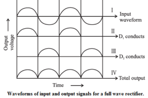
The output voltage has a fixed polarity but varies periodically with time between zero and a maximum value. Above figure shows the input and output voltage waveforms. The pulsating dc output voltage of a full− wave rectifier has twice frequency of the input.
Question 6. Explain how a Zener diode maintains constant voltage across a load.
Zener diode as a voltage regulator
Principle : In the breakdown region of a Zener diode, for widely changing Zener current, the voltage across the Zener diode remains almost constant.
Electric circuit : The circuit for regulating or stabilizing the voltage across a load resistance RL against change in load current and supply voltage is shown in Fig.
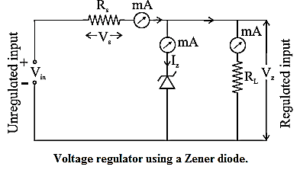
The Zener diode is connected parallel to load RL such that the current through the Zener diode is from the n to p region. The series resistance RS limits the current through the diode below the maximum rated value.
From the circuit, I = IZ + IL and V = IRS + VZ = (IZ + IL)RS + VZ
Working of a Zener Regulator :
- When the input unregulated dc voltage V across the Zener diode is greater than the Zener voltage VZ in magnitude, the diode works in the Zener breakdown region. The voltage across the diode and load RL is then VZ. The corresponding current in the diode is IZ.
- As the load current (I) or supply voltage (V) changes, the diode current (IZ) adjusts itself at constant VZ. The excess voltage V—VZ appears across the series resistance RS.
- For constant supply voltage, the supply current I and the voltage drop across Rs remain constant. If the diode is within its regulating range, an increase in load current is accompanied by a decrease in IZ at constant VZ.
- Since the voltage across RL remains constant at VZ, the Zener diode acts as a voltage stabilizer or voltage regulator.
Question 7. Explain the forward and the reverse characteristic of a Zener diode.
forward and the reverse characteristic of a Zener diode :
- The forward bias region of a Zener diode is identical to that of a regular diode. There is forward current only after the barrier potential of the pn− junction is overcome. Beyond this threshold or cut in voltage, there is an exponential upward swing.
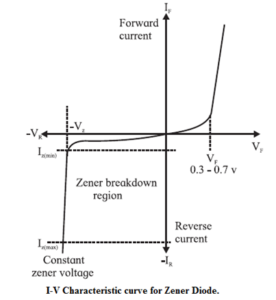
- The typical forward voltage at room temperature with a current of around 1 mA is around 0.6 V.
- In the reverse bias condition the Zener diode is an open circuit and only a small reverse saturation current flows as shown with change of scale. At the reverse breakdown voltage there is an abrupt rapid increase in the current− the knee is very sharp, followed by an almost vertical increase in current.
- The voltage across the Zener diode in the break− down region is very nearly constant with only a small increase in voltage with increasing current.
- There is a minimum Zener current, IZ (min), that places the operating point in the desired break− down region. At some high current level, IZM, the power dissipation of the diode becomes excessive beyond which the diode can be damaged.
Question 8. Explain the working of a LED.
Working :
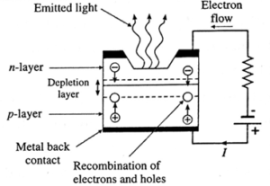
- A forward− biased LED operates between 1.2 and 3.6 V at 12 to 20 mA. In the active layer, the majority of carriers inject holes from the p− type layer and electrons from the n− type layer.
- Electrons enter the p− layer through the junction. Some of these surplus minority carriers, electrons, merge radiatively with majority carriers, holes, in the active p− layer, producing photons as a byproduct.
- The energy of the ensuing photon is about equivalent to the active layer material's bandgap. Changing the active layer's bandgap produces photons with various energy.
- In the energy band diagram this recombination is equivalent to a transition of the electron from a higher energy state in the conduction band to a lower energy state in the valence band. The energy difference is emitted as a photon of energy hν.
Question 9. Explain the construction and working of solar cell.
Construction of a Solar Cell:
- A p− type semiconductor substrate is backed by a metal electrode back contact in a simple pn− junction solar cell.
- By doping with an appropriate donor impurity, a thin n− layer (less than 2.5 pm for silicon) is created over the p− type substrate.
- Metal finger electrodes are formed on top of the n− layer, leaving enough space between the fingers for sunlight to reach the n− layer and, ultimately, the underlying pn− junction.
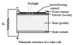
Working : When exposed to sunlight, the absorption of incident radiation (in the range near− UV to infrared) creates electron− hole pairs in and near the depletion layer.
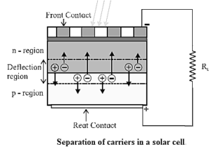
- Consider light of frequency v incident on the pn− junction such that the incident photon energy hv is greater than the band gap energy EC of the semiconductor.
- The photons excite electrons from the valence band to the conduction band, leaving vacancies or holes in the valence band, thus generating electron—hole pairs.
- The photogenerated electrons and holes move towards the n side and p side, respectively. If no external load is connected, these photogenerated charges get collected at the two sides of the junction and give rise to a forward photo− voltage.
- In a closed− circuit, a current I passes through the external load as long as the solar cell is exposed to sunlight.
- A solar cell module consists of several solar cells connected in series for a higher voltage output.
- For outdoor use with higher power output, these modules are connected in different series and parallel combinations to form a solar cell array.
Question 10. Explain the principle of operation of a photodiode.
- A photodiode is operated in the reverse bias mode which results in a wider depletion region.
- When operated in the dark (zero illumination), there is a reverse saturation current due solely to the thermally generated minority charge carriers. This is called the dark current. Depending on the minority carrier concentrations, the dark current in an Si photodiode may range from 5 pA to 10 nA.
- When exposed to radiation of energy hv 2 EC (in the range near− UV to near− IR), electron− hole pairs are created in the depletion region.
- The electric field in the depletion layer accelerates these photo− generated electrons and holes towards the n side and p side, respectively, constituting a photocurrent I in the external circuit from the p side to the n side.
- Due to the photogeneration, more charge carriers are available for conduction and the reverse current is increased. The photocurrent is directly proportional to the intensity of the incident light. It is independent of the reverse bias voltage.
Question 11. What do you mean by a logic gate, a truth table and a Boolean expression?
(a) Logic gate : A logic gate is a basic switching circuit used in digital circuits that determines when an input pulse can pass through to the output. It generates a single output from one or more inputs.
(b) Truth table : The table which shows the truth values of a Boolean expression for a logic gate for all possible combinations of its inputs is called the truth table of logic gate.
The truth table contains one row for each input combination. Since a logical variable can assume only two possible values, 0 and 1, there are 2N combinations of N inputs so that the table has 2 N rows.
(c) The mathematical statement that provides the relationship between the input and the output of a logic gate is called a Boolean expression.
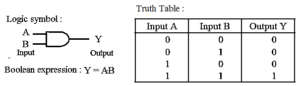
Question 12. What is logic gate? Write down the truth table and Boolean expression for ‘AND’ gate.
Logic gate : A logic gate is a basic switching circuit used in digital circuits that determines when an input pulse can pass through to the output. It generates a single output from one or more inputs.
AND gate :
It is a circuit with two or more inputs and one output in which the output signal is HIGH if and only if all the inputs are HIGH simultaneously.
The AND operation represents a logical multiplication.
Figure shows the 2− input AND gate logic symbol and the Boolean expression and the truth table for the AND function.
Question 13. What are the uses of logic gates? Why is na NOT gate known as an inverter?
Uses :
- Any digital computation method involves conducting a series of arithmetic operations on the problem's data.
- The type of the operation to be done at each stage in the calculation is dictated partly by the pre− specified programme and partly by the results of previous stages in the process.
- To perform logical processes, we need switches with many inputs, i.e., the outputs of these switches are determined in certain ways by the condition (binary state) of their inputs. These configurations are known as logic gates, and they are typically an expansion of a simple transistor switch.
A logic gate can be represented by its logic symbol, Boolean expression and the truth table.
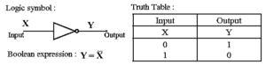
NOT gate or INVERTER :
It is a circuit with one input whose output is HIGH if the input is LOW and vice versa.
The NOT operation outputs an inverted version of the input. Hence, a NOT gate is also known as an INVERTER.
The small invert bubble on the output side of the inverter logic symbol,
Fig. and the over bar (—) in the Boolean expression represent the invert function.
Question 14. Write the Boolean expression for (i) OR gate, (ii) AND gate, and (iii) NAND Gate.
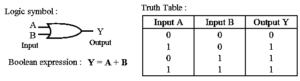
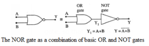
(i) OR gate : It is a circuit with two or more inputs and one output in which the output signal is HIGH if any one or more of the inputs is HIGH.
The OR operation represents a logical addition.
Fig. shows the 2− input OR gate logic symbol, and the Boolean expression and the truth table for the OR function.
(ii) NOR gate : It is a circuit with two or more inputs and one output, in which the output is HIGH if and only if all the inputs are LOW.
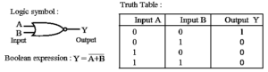
The NOR gate is realized by connecting the output of OR gate to the input of a NOT gate, so that the truth table of the NOR function is obtained by inverting the outputs of the OR gate.
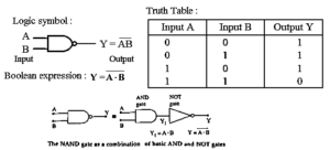
(iii) NAND gate : It is a circuit with two or more inputs and one output, whose output is HIGH if any one or more of the inputs is LOW; the output is LOW if all the inputs are HIGH.
The NAND gate is a combination of an AND gate followed by a NOT gate so that the truth table of the NAND function is obtained by inverting the outputs of the AND gate.
Question 15. Why is the emitter, the base and the collector of a BJT doped differently?
- A BJT being a bipolar device, both electrons and holes participate in the conduction process.
- Under the forward− biased condition, the majority carriers injected from the emitter into the base constitute the largest current component in a BJT.
- For these carriers to diffuse across the base region with negligible recombination and reach the collector junction, these must overwhelm the majority carriers of opposite charge in the base.
- The total emitter current has two components, that due to majority carriers in the emitter and that due to minority carriers diffused from base into emitter.
- The ratio of the current component due to the injected majority carriers from the emitter to the total emitter current is a measure of the emitter efficiency.
- To improve the emitter efficiency and the common− base current gain (x), it can be shown that the emitter should be much heavily doped than the base.
- Also, the base width is a function of the base− collector voltage. A low doping level of the collector increases the size of the depletion region. This increases the maximum collector− base voltage and reduces the base width.
- Further, the large depletion region at the collector− base junction− extending mainly into the collector− corresponds to a smaller electric field and avoids avalanche breakdown of the reverse− biased collector− base junction.
Question 16. Which method of biasing is used for operating transistor as an amplifier?
For use as an amplifier, the transistor should be in active mode. Therefore, the emitter− base junction is forward biased and the collector− base junction is reverse biased. Also, an amplifier uses an emitter bias rather than a base bias.
Question 17. Define α and β. Derive the relation between then.
The dc common-base current ratio or current gain (αdc) is defined as the ratio of the collector current to emitter current.
αdc = IC/IE
The dc common-emitter current ratio or current gain (βdc) is defined as the ratio of the collector current to base current.
βdc = IC/IB
Since the emitter current IE =IB + IC,
IE/IC = IB/IC + 1
∴ \(\frac{1}{α_{dc}}=\frac{1}{β_{dc}}+1\)
Therefore, the common—base current gain in terms of the common-emitter current gain is
αdc = \(\frac{β_{dc}}{1+β_{dc}}\)
and the common-emitter current gain in terms of the common-base current gain is
βdc = \(\frac{α_{dc}}{1-α_{dc}}\)`
Since the electrical relationship between these three currents IB, IC and IE is determined by the physical construction of the transistor itself, any small change in the base current (IB), will result in a much larger change in the collector current (IC). Thus, a small change in current flowing in the base will control the current in the emitter− collector circuit.
Question 18. The common− base DC current gain of a transistor is 0.967. If the emitter current is 10mA. What is the value of base current.
Given : IE = 10 mA, IC = 9.8 mA
IE = IB + IC
Therefore, the base current,
IB = IE − IC = 10 – 9.8 = 0.2 mA
Question 19. In a comman− base connection, a certain transistor has an emitter current of 10mA and collector current of 9.8 mA. Calculate the value of the base current.
Given : αdc =0.967, IE = 10 mA
We know, αdc = \(\frac{I_C}{I_E}\)
Therefore, the collector current,
IC = αdcIE = 0.967 x 10 = 9.67mA
Therefore, the base current,
IB = IE − IC = 10 − 9.67 = 0.33 mA
Question 20. In a common− base connection, the emitter current is 6.28 mA and collector current is 6.20 mA. Determine the common base DC current gain.
Given : IE = 6.28 mA, IC = 6.20 mA
Common− emitter current gain, αdc = \(\frac{I_C}{I_E}\) = \(\frac{6.20}{6.28}\) = 0.9873
IE = IB + IC
Therefore, the base current,
IB = IE − IC = 6.28 – 6.20 = 0.08 mA
Common− base current gain, βdc = \(\frac{I_C}{I_B}\) = \(\frac{6.20}{0.08}\) = 77.5
[Note: The solution in the textbook clearly relates to the common− emitter current gain.]
We reply to valid query.