Notes-Part-2
Topics to be Learn : Part-2
|
Packing efficiency : Packing efficiency is the fraction or a percentage of the total space occupied by the spheres (particles).
The magnitude of packing efficiency gives a measure of how tightly particles are packed together.
Packing efficiency = \(\frac{\text{Volume occupied by particles in unit cell}}{\text{total volume of unit cell}}×100\)
Packing efficiency of metal crystal in simple cubic lattice :
Step 1 : Radius of sphere : In simple cubic unit cell, particles (spheres) are at the corners and touch each other along the edge.

A face of simple cubic unit cell is shown in Fig. It is evident that
a = 2r or r = a/2 ………(1)
where r is the radius of atom and ‘a’ is the length of unit cell edge.
Step 2 : Volume of sphere : Volume of a sphere = .\(\frac{4π}{3}×r^3\)
Substitution for r from Eq. (1)
∴ Volume of one particle = \(\frac{4π}{3}(\frac{a}{2})^3\) = \(\frac{πa^3}{6}\)
Step 3 : Total volume of particles : Because simple cubic unit cell contains only one particle, volume occupied by particle in unit cell = \(\frac{πa^3}{6}\)
Step 4 : Packing efficiency
Packing efficiency = \(\frac{\text{Volume occupied by particles in unit cell}}{\text{total volume of unit cell}}×100\)
= \(\frac{πa^3/6}{a^3}×100 = \frac{π}{6}×100=\frac{3.142}{6}×100 \)
= 52.36%
Thus, in simple cubic lattice, 52.36 % of total space is occupied by particles and 100−52.36 = 47.64 % is empty space,
∴ void volume or a percentage of void space=.47.64 %
Packing efficiency of metal crystal in body-centred cubic lattice :
Step 1 : Radius of sphere (particle) : In the unit cell of body-centred cubic lattice, there are 8 atoms (particle) at 8 comers and one atom at the centre of the cube.

Figure shows that the particle at the centre of the cube touches two corner particles along the diagonal of the cube.
To obtain radius of the particle (sphere) Pythagorus theorem is applied.
- For triangle FED, ∠ FED = 900.
∴ FD2 = FE2 + ED2 = a2 +a2 = 2a2 (because FE = ED = a) …….(1)
- For triangle AFD, ∠ ADF = 900
∴ AF2 = AD2 + FD2 ……..(2)
Substitution of Eq. (1) into Eq. (2) yields
AF2 = a2 + 2a2 = 3a2 (because AD = a)
∴ AF = \(\sqrt{3}a\) ………(3)
The Fig. shows that AF = 4r.
Substitution for AF from equation (3) gives
∴ \(\sqrt{3}a\) = 4r
∴ r = \(\frac{\sqrt{3}}{4}a\) ….. (4)
Step 2 : Volume of sphere : Volume of sphere particle = \(\frac{4π}{3}×r^3\),
Substitution for r from Eq. (4),
∴ Volume of one particle = .\(\frac{4π}{3}(\frac{\sqrt{3}}{4}a)^3 \) = \(\frac{\sqrt{3}πa^3}{16}\)
Step 3 : Total volume of particles : Unit cell bcc contains 2 particles. Hence, volume occupied by particles in bcc unit cell = 2 ×
= 2 × \(\frac{\sqrt{3}πa^3}{16}\) = \(\frac{\sqrt{3}πa^3}{8}\)
Step 4 : Packing efficiency
Packing efficiency = \(\frac{\text{Volume occupied by particles in unit cell}}{\text{total volume of unit cell}}×100\)
= \(\frac{\sqrt{3}πa^3/8}{a^3}×100\) = 68 %
Thus, 68% of the total volume in bcc unit lattice is occupied
∴ Percentage of void space = 100 − 68 = 32 %
Packing efficiency of metal crystal in face-centred cubic lattice (or ccp or hcp lattice)
Step 1 : Radius of particle/sphere : The corner particles are assumed to touch the particle at the centre of face ABCD as shown in Fig.
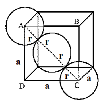
The triangle ABC is right angled with ∠ABC = 900. According to Pythagorus theorem,
AC2 = AB2 + BC2 = a2 +a2 = 2a2
(because AB = BC = a)
Hence, AC = \(\sqrt{2}a\) …. (1)
From figure AC = 4 r. Substitution for AC from Eq. (1.) gives
\(\sqrt{2}a\) = 4r
∴ r = \(\frac{\sqrt{2}}{4}a = \frac{a}{2\sqrt{2}}\) ….(2)
Step 2 : Volume of sphere : Volume of one particle = \(\frac{4π}{3}×r^3\)
Substitution for r from Eq. (2)
∴ Volume of one particle = \(\frac{4π}{3}× (\frac{a}{2\sqrt{2}})^3\)
= \(\frac{4πa^3}{3}× (\frac{1}{2\sqrt{2}})^3\)
= \((\frac{πa^3}{12\sqrt{2}})^3\)
Step 3 : Total volume of particles : The unit cell of fcc lattice contains 4 particles. Hence, volume occupied by particles in fcc unit cell
= 4 × \((\frac{πa^3}{12\sqrt{2}})^3\)
= \((\frac{πa^3}{3\sqrt{2}})^3\)
Step 4 : Packing efficiency :
Packing efficiency = \(\frac{\text{Volume occupied by particles in unit cell}}{\text{total volume of unit cell}}×100\)
= \(\frac{πa^3/3\sqrt{2}}{(a^3)}×100\) = \(\frac{3.142}{3\sqrt{2}}×100\) = 74 %
Thus in fcc/ccp/hcp crystal lattice, 74% of the total volume is occupied by particles
∴ Percentage of void space = 100 −74 = 26 %
Q. Which of the three types of packing used by metals makes the most efficient use of space and which makes the least efficient use ?
Ans. fcc has the most efficient packing of particles awhile scc has the least eflicient packing.
Below Table shows the expressions for various parameters of particles in terms of unit cell dimension for cubic systems.

Below Table shows the summary of coordination number of particles and packing efficiency in various cubic systems.

Number of particles and unit cells in ‘x’ g of metallic crystal :
Consider ‘x’ gram of a metallic crystal of molar mass M and density ρ.
If the unit cell of the crystal has edge length ‘a’ then, volume of unit cell = a3.
ρ = \(\frac{mass}{volume}\)
= \(\frac{\text{ no of particles in unit cell}}{\text{volume of unit cell}}×\frac{M}{N_A}\)
∴ ρ =\( \frac{n}{a^3}\) ×\frac{M}{N_A}\)
∴ M = \( \frac{ρa^3N_A}{n}\) \)
where 'n' is the number of particles in unit cell and 'a3' is the volume of unit cell.
i. Number of particles in 'x' g metal :
∴ Molar mass, M, contains NA particles
∴ x g of metal contains\(\frac{xN_A}{M}\) particles
substitution of M gives
Number of particles in 'x' g = \(\frac{xN_A}{ρa^3N_A/n}\) = \(\frac{xn}{ρa^3}\)
ii. Number of unit cells in 'x' g metal :
∴ 'n' particles correspond to 1 unit cell
∴ \(\frac{xn}{ρa^3}\) particles correspond to \(\frac{xn}{ρa^3}×\frac{1}{n}\) unit cells.
∴ Number of unit cells in 'x' g metal = \(\frac{x}{ρa^3}\)
iii. Number of unit cells in volume 'V' of metal = \(\frac{V}{a^3}\)
Crystal defects or imperfections : The real, naturally occurring crystalline substances do not have perfect crystal structures. They have some disorders or irregularities in the stacking of atoms. Such irregularities in the arrangement of constituent particles of a solid crystal are called defects or imperfections.
- Defect in crystalline structure : Any deviation from orderly and stoichiometrically perfect arrangement of atoms, ions or molecules in the crystal lattice is called a defect in the crystalline structure.
- Defects are created during the crystallization process. If the process occurs at faster rate, the defects are more.
- The properties of solids are affected due to imperfections.
There are three types of defects: point defects, line defects and plain defects. Only point defects will be discussed in this chapter.
Point defects : These defects arise due to irregularities produced in the arrangement of basis of lattice points in crystalline solids.
There are three major classes of point defects :
- stoichiometric point defects,
- impurity defects
- non-stoichiometric point defects.
a. Stoichiometric point defects : Chemical formula of a compound shows fixed ratio of number of atoms or number of cations and anions. This fixed ratio is the stoichiometry of the compound.
In stoichiometric defect, the stoichiometry remains unchanged. In other words, the ratio of number of atoms or number of cations and anions of compound remains the same as represented by its chemical formula.
There are four types of stoichiometric point defects as
- vacancy defect,
- self interstitial defect,
- Schottky defect
- Frenkel defect.
Vacancy defect :

- During crystallisation, some of regular sites in solid remain unoccupied and the missing particle creates a vacancy defect.
- The defect can be developed by heating the substance.
- The mass of solid decreases due to absence of particles in regular sites.
- Since the volume remains the same the density of the substance decreases.
Self Interstitial defect in elemental solid :
The empty spaces or voids in between the particles at lattice points represent interstitial defective sites or self interstitial defects.
This defect arises in the following two ways :
(1) An extra particle occupies the empty interstitial space. This extra particle is similar to those already present in the crystal.

(2) A particle gets shifted from its original regular site to an empty interstitial space in the crystal.

- This displacement of a particle produces a vacancy defect at its regular site.
- This defect is referred to as a combination of vacancy defect and self-interstitial defect.
- Since there is neither loss or gain in mass of the substance, the density of it remains unchanged-
Schottky defect :

- Schottky defect arises in ionic solids due to missing of equal number of cations and anions from their regular positions in the crystal lattice creating vacancies.
- There arises formation of two holes per loss of ion pair.
Conditions for formation of Schottky defect :
Characteristics of ionic solids showing Schottky defect :
- High degree of ionic character
- High coordination number of anion
- Small difference between ionic size or radii of cation and anion. The ionic ratio is not below unity.
Consequences of Schottky defect
- As the number of ions decreases, mass decreases. However, volume remains unchanged. Hence, the density of a substance decreases.
- The number of missing cations and anions is equal, the electrical neutrality of the compound is preserved.
- This defect is found in ionic crystals such as NaCl, AgBr and KCl.
Frenkel defect : This defect arises when an ion of an ionic compound is missing from its regular site and occupies interstitial vacant position between lattice points.

- Cations have smaller size than anions, hence generally cations occupy the interstitial sites.
- This creates a vacancy defect at its original position and interstitial defect at new position.
- Frenkel defect is regarded as the combination of interstitial defect and vacancy defect.
Conditions for the formation of Frenkel defect :
- This defect arises in ionic compounds with a large difference between the sizes of cation and anion.
- The ionic compounds must have ions with low coordination number.
Consequences of Frenkel defect :
- As no ions are missing from the crystal lattice as a whole, the density of solid and its chemical properties remain unchanged.
- The crystal as a whole remains electrically neutral because the equal numbers of cations and anions are present.
- This defect is found in ionic crystals like ZnS, AgCl, AgBr, AgI, CaF2.
Impurity defect : This defect arises when foreign atoms, that is, atoms different from the host atoms are present in the crystal lattice.
There are two types of impurity defects namely
(1) Substitutional defects and (2) Interstitial defects.
i. Substitutional impurity defect : In this defect, the foreign atoms are found at the lattice sites in place of host atoms. The regular atoms are displaced from their lattice sites by impurity atoms.
For example : Solid solutions of metals (alloys) : Brass is an alloy of Cu and Zn. In brass, host Cu atoms are replaced by impurity of Zn atoms. The Zn atoms occupy regular sites of Cu atoms as shown in Fig.

Vacancy through aliovalent impurity :
By addition of impurities of aliovalent ions

When aliovalent ion like Sr2+ in small amount is added by adding SrCl2 to NaCl during its crystallisation, each Sr2+ ion (oxidation state 2 +) removes 2 Na+ ions from their lattice points, to maintain electrical neutrality. Hence one of vacant lattice site is occupied by Sr2+ ion while other site remains vacant.
ii. Interstitial impurity defect :

A defect in solid in which the impurity atoms occupy interstitial vacant spaces of lattice structure is called interstitial impurity defect.
For example, in steel, normal lattice sites are occupied by Fe atoms but interstitial spaces are occupied by carbon atoms. .
Nonstoichiometric defects :
Nonstoichiometric defect arises when the ratio of number of atoms of one kind to that of other kind or the ratio of number of cations to anions becomes different from that indicated by its chemical formula. i.e. stoichiometry of the compound is changed.
- The change in stoichiometry does not cause any change in the crystal structure.
- There are two types of nonstoichiometric defects
i. Metal deficiency defect : This defect arises in compounds of metal which show variable oxidation states. In some metal crystals, positive metal ions are missing from their regular lattice sites.
The extra negative charge is balanced by cations of the same metal with higher oxidation state than that of missing cation at site.

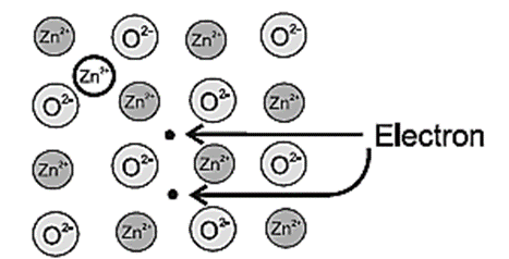
For example, in the compound NiOone Ni2+ ion is missing creating a vacnacy at its lattice site. The deficiency of two positive charges is made up by the presence of two Ni3+ ions at the other lattice sites of Ni2+ ions as shown in Fig. The composition of NiO then becomes Ni0.97O1.0
ii. Metal excess defect : There are two types of metal excess defect as follows :
(a) Presence of a neutral atom or an extra positive ion at interstitial position :
There are two types or ways of metal excess defects in ZnO. In the first case, Zn atom is present in the interstitial space as shown in figure.

(b) Metal ions and electrons at interstitial sites :
The second case arises when ZnO is heated,
Zn2+ and electrons are obtained,
ZnO → Zn2+ + ½O2 + 2e−
The excess Zn2+ ions are trapped in interstitial site in the lattice. The electrons also diffuse in the crystal to occupy interstitial sites as shown in Fig.
In both the cases, nonstoichiometric formula of ZnO is Zn1+xO1.0
Defects due to anion vacancies OR colour of crystals or F centres :
The defect due to anion vacancies imparts colour to the colourless crystal.
- When a colourless crystal of NaCl is heated in the atmosphere of sodium vapour, the sodium atoms are deposited on the crystal surface.

- Due to diffusion of Cl- ions to the crystal surface vacancies are created at their regular sites.
- These diffused Cl- ions combine with Na atoms on the surface forming NaCl along with releasing electrons from sodium atoms.
- Na + Cl- → NaCl + e-
- The released electrons diffuse into the crystal and occupy vacant sites of anions Cl- in the crystal.
- The anion vacant sites occupied by electrons are called F-centres or colour centres. Due to colour centres NaCl shows yellow colour.
- Now NaCl crystal has excess of Na atoms having nonstoichiometric formula Na1+xCl1.0
Q. When ZnO is heated it turns yellow and returns back to original white colour on cooling. What could be the reason ?
- When colourless ZnO is strongly heated, the metal atoms are deposited on crystal surface and anions O2- migrate to the surface producing vacancies at anion lattice points.
- These anions combine with Zn atoms forming ZnO and release electrons.
- Zn + O2- —> ZnO + 2e-
- These released electrons diffuse into the crystal and occupy vacant sites of anions and produce F-centres.
- Due to these colour centres, ZnO turns yellow.
Electrical properties of solids :
Solids show very wide range of electrical conductivity. According to electrical conductivity, solids are classified as follows :
(i) Conductors :
- The solids having electrical conductivity in the range of 104 to 107 Ohm-1m-1 are called conductors.
- The examples of conductors are metals and electrolytes.
- Electrical conductivity in metals is due to free movement of electrons while electrolytes conduct electricity due to migration ions.
(ii) Insulators :
- Solids having low electrical conductivities in the range 10-20 to 10-10 Ohm-1m-1 are called insulators.
- Examples : Nonmetals and molecular solids belong to this category.
(iii) Semiconductors :
- Solids having electrical conductivities in the range 10-6 to 104 Ohm-1m-1 are semiconductors.
- This range is intermediate between conductors and insulators.
- For Examples : Metalloids like silicon, germanium belong to this category.
Band theory (origin of electrical properties in solids) : Electrical conductivities of solid metals, nonmetals and metalloids are explained in terms of band theory, which involves the presence of free electrons.
- According to band theory, the atomic orbitals of metal atoms overlap to form molecular orbitals which are spread all over the crystal structure.
- The energy difference between adjacent molecular orbitals decreases as the number of molecular orbitals increases and when it becomes very less, the orbitals merge into one another forming continuous bands which extent over the entire crystal.
There are two types of bands of molecular orbitals s follows :
- Valence band : The atomic orbitals with filled electrons from the inner shells form valence bands, where there are no free mobile electrons since they are involved in bonding.
- Conduction band : Atomic orbitals which are partially filled or empty on overlapping form closely placed molecular orbitals giving conduction bands where electrons are delocalised and can conduct, heat and electricity.
Band gap : The energy difference between valence band and conduction band is called band gap.
- Band gap decides whether electrons from valence band can be promoted to vacant conduction band or not.
- The conductors like metals have very small or no band gap and electron can be promoted by thermal energy. The nonconductors have large band gap. The insulators have very large band gap.
The band gap energy values of a few solids are as shown here.

Metals :
- Metals are good conductors of electricity since the outermost electrons of all the atoms in the metallic crystal occupy conduction band.
- The number of electrons in conduction bands is very large.

- The conduction bands in metals can be labelled as ‘s’ band, overlapping s and p bands etc. according to overlapping of orbitals.
- This results in delocalisation of outermost electrons forming metal ions. Hence, this is analogous to metal cations immersed in the sea of electrons.
Q. Why does metallic conductivity decrease by increasing temperature ?
- In metals a large number of outermost electrons of atoms occupy conduction bands.
- Band formation in metals results in delocalisation of outennost electrons forming metal ions or cations.
- The metallic cations occupying crystal lattice sites vibrate about mean positions.
- As temperature increases the vibrational motion increases which interrupts flow of electrons decreasing electrical conductivity.
| Extra note :
• Metallic sodium is an example of conductor where the conduction band is partially filled and there is no band gap. Electronic configuration of Na is [Ar]3s1. Interaction of the partially filled 3s AOs of all the Na atoms gives rise to same number of MOs. All these closely spaced MOs together form a continuous band of energies which is called 3s band. Lower half of 3s band corresponds of BMOs and is filled while the upper half of 3s band corresponds to AMOs and is empty. There is no gap between these two halves. The 3s band in sodium is the conduction band which contains same number of electrons as the sodium atoms. This is responsible for the high conductivity of metallic sodium. • Metallic magnesium is an example of conductor with overlapping bands. Electronic configuration of Mg is [Ar]3s23p0. Interaction of completely filled 3s AOs of all the Mg atoms gives rise to the same number of MOs all of which are filled. These together form the 3s band which is a completely filled band. Interaction of vacant 3p AOs of all the Mg atoms gives rise to the same number of vacant MOs together called 3p band. This is the vacant band. The filled 3s band and vacant 3p band overlap each other. As a result, higher energy electrons move from 3s band to 3p band. |
Insulators : In insulators the valence band is completely filled by electronics while conduction band is empty.

- The energy gap between valence band and conduction band in insulator is very large.
- Thermal energy is not sufficient to promote electrons from valence band to conduction band.
- Therefore, the conduction band in insulator remains vacant and does not allow the conduction of electricity.
Semiconductors : Electrical conductivity of a semiconductor material is intermediate between that of metals and insulators.

- The substances like silicon, germanium which have poor electrical conductance at low temperature but the conductance increases with the increase in temperature are called semi-conductors.
- The energy difference between valence band and conduction band is relatively small, hence the electrons from valence band can be excited to conduction band by heating.
Types of semiconductors : There are two types of semiconductors :
- Intrinsic semiconductor
- Extrinsic semiconductor
(a) Intrinsic semiconductor :
- A pure semiconductor material like pure Si, Ge which have a very low but finite electrical conductivity is called intrinsic semiconductor.
- The electrical conductivity of a semiconductor increases with the increase in temperature.
(b) Extrinsic semiconductor :
- Semiconductor doped with different element is called extrinsic semiconductor.
- By doping with elements like Ga or P, the electrical conductivity is increased.
| Remember...
Electrical conductivity of metals decreases and that of semiconductor increases with increasing temperature. |
Extrinsic semiconductors and doping :
Doping : The conductivity of a semiconductor can be increased by doping. The process of addition of minute quantity of impurities to a semiconductor to increase its conductivity is called doping. The added impurity is called dopant.
Extrinsic semiconductors : A doped semiconductor, having higher conductivity than pure intrinsic semiconductor, is an extrinsic semiconductor.
- A semiconductor obtained by doping intrinsic semiconductor with elements of third group and fifth group is called extrinsic semiconductor.
- This extrinsic semiconductor has higher electrical conductivity than pure intrinsic semiconductor.

There are two types of extrinsic semiconductors :
(A) n-type semiconductor :
- n-type semiconductor contains increased number of electrons in the conduction band.
- When Si semiconductor is doped with 15th group element phosphorus, P, the new atoms occupy some vacant sites in the lattice in place of Si atoms.

- P has five valence electrons, out of which four are involved in covalent bonding with neighbouring Si atoms while one electrons remains free and delocalised.
- These free electrons increase the electrical conductivity of the semiconductor.
- The semiconductors with extra non-bonding free electrons are called n-type semiconductors.
(B) p-type semiconductor :
- p-type semiconductor is obtained by doping a pure semiconductor by an element of 13th group like B.
- 13th group element has less number of valence electrons. When pure Si is doped with B atoms, these atoms occupy Si lattice points.

- Boron (SB) has only 3 valence electrons which form covalent bonds with the neighbouring Si atoms, while one bond has shortage of one electron.
- This creates a vacancy or a hole, hence the electron from neighbouring Si atom jumps into this hole creating a vacancy in itself. This process continues, i.e., positive holes move in one direction while electrons moves inopposite direction.
- Due to electron deficient positions, this semiconductor is called p-type semiconductor.
- When p-type semiconductor is connected to the external source of electricity, electrons from neighbouring silicon atoms jump into the holes so that electrons move towards positive electrode and holes migrate towards negative electrode.
- Hence electrical conduction in p-type semiconductor is due to electrons and holes.
| Remember :
• Whether intrinsic or extrinsic semiconductor, the material is electrically neutral. • An n-type semiconductor such as Si doped with P has more electrons than those needed for bonding and thus has electrons in the partially filled conduction band. • A p-type semiconductor such as Si doped with B has the less electrons than needed for bonding and thus has vacancies (holes) in the valence band. Activity : If a small quantity of phosphorus be doped into pure silicon.
|
Uses of semiconductors :
- They are used in transistors, digital computers and cameras.
- They are used in solar cells and television sets.
- By combining n-type and p-type semiconductors, n-p junctions are formed which are effectively used in rectifiers or to convert light energy into electrical energy.
Magnetic properties of solids : Magnetic properties of solids can be understood easily in terms of classical picture of electron.
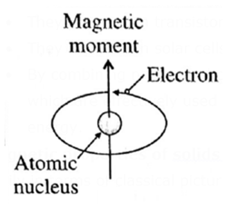
- The electrons spin about their own axis. The spinning electrons act like tiny magnets because their spinning action generates induced magnetic field.
- If an orbital contains one electron, the unbalanced spin exhibits magnetism.
- However, when electrons are paired their spin is balanced and no magnetic property is observed.
On the basis of magnetic properties solids are classified into three major classes : diamagnetic, paramagnetic and ferromagnetic.
Diamagnetism :
The magnetic properties of a substance arise due to presence of the electrons.
An electron while revolving around the nucleus, also spins around its own axis and generates a magnetic moment and a magnetic property.
- If an atom or a molecule of the substance contains all electrons paired, spinning clockwise and anticlockwise, their magnetic moments and magnetic properties get cancelled. Hence they oppose and repel the applied magnetic field. This phenomenon is called diamagnetism and the substance is said to be diamagnetic.

- N2, F2, NaCl, H2O and benzene are some examples of diamagnetic substances.
Paramagnetism: (Paramagnetic substances) :
The magnetic properties of a substance arise due to the presence of electrons.
An electron while revolving around the nucleus, also spins around its own axis and generates a magnetic moment and magnetic properties.
- If an atom or a molecule contains one or more unpaired electrons spinning in same direction, clockwise or anticlockwise, then the substance is associated with net magnetic moment and magnetic properties. They experience a net force of attraction when placed in the magnetic field. This phenomenon is called paramagnetism and the substance is said to be paramagnetic.
- For example : Oxygen, Cu2+, Fe3+, Cr3+ are some examples of paramagnetic substances.
Ferromagnetism :
- The substances containing large number of unpaired electrons are attracted strongly by magnetic field. These substances are said to be ferromagnetic.
- These substances can be permanently magnetised. They retain magnetism even after the removal of external magnetic field.
- In the solid state, the metal ions of ferromagnetic substance are grouped together into small regions called domains, where each domain acts as a tiny magnet.
- Some example of ferromagnetic substances are Fe, Co, Ni, Gd, CrO2.
We reply to valid query.