Notes Part-1
|
Topics to be Learn : Part -1
|
Introduction:
- Conductors such as metals have a very high electrical conductivity, of the order of 107 Sm—1.
- insulator or a bad conductor like glass has a very low electrical conductivity of the order of 10—10 Sm—1.
- Electrical conductivity of a semiconductor lies between that of a good conductor and a bad conductor.
- A semiconductor can be customised to have its electrical conductivity as per our requirement. Temperature dependence of electrical conductivity of a semiconductor can also be controlled.
Electrical conduction in solids:
Charge carrier : Charge carriers are particles that carry an electric charge and may move freely inside a substance. Electrical conduction occurs when charged particles are transported through a solid by an external electric field.
Electrical conduction in a solid depends upon,
- its temperature,
- the number of charge carriers,
- how easily these carries can move inside a solid (mobility),
- its crystal structure,
- types and the nature of defects present in a solid etc.
(i) Conductors (Metals):
- In a metal, the outermost electrons in an atom are loosely bound to the nucleus and are readily available for electrical conduction. Such electrons are called free electrons.
- These electrons act as charge carriers in the metallic structure, thus allowing an electric current through the metal.
- Due to a large number of such electrons (nearly 1028 electrons per m3) present in them, the metals are good conductors of electricity.
(ii) Insulators: Glass, wood or rubber are some common examples of insulators. Insulators have very small number (1023 per m3) of free electrons.
(iii) Semiconductors:
The electrical conductivity of a semiconductor is between the conductivity of a metal and that of an insulator
Figure shows the temperature dependence of the electrical conductivity of a typical metal and a semiconductor.

- When the temperature of a semiconductor is increased, its electrical conductivity also increases.
- The electrical conductivity of a metal decreases with increase in its temperature.
Semiconductors can be broadly classified as :
- Elemental semiconductors : silicon, germanium
- Compound semiconductors : cadmium sulphide, gallium arsenide, zinc sulphide
- Organic semiconductors : anthracene, doped phthalocyanines, polyaniline.
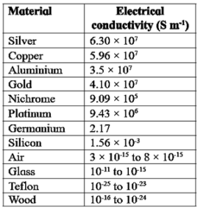
Electrical conductivities of some commonly used materials :
[Know This : Elemental semiconductors and compound semiconductors are widely used in electronic industry. Discovery of organic semiconductors is relatively new and they find lesser applications.]
Band theory of solids, a brief introduction:
Energy band : At the equilibrium interatomic separation, the interaction of the atoms in a crystal separates each of the discrete permissible atomic energy levels into a quasi-continuous band of allowed energy levels separated by an exceedingly tiny energy difference, roughly 10—19 eV. Such a band of allowed energies is called an energy band.
Pauli’s exclusion principle :
No two electrons in an atom may have the same set of quantum numbers (n, l, ml, and ms). OR No two comparable spin electrons in an atom may be in the same quantum state.
[n = the total quantum number, l= the orbital quantum number, ml = the magnetic quantum number, ms = the spin magnetic quantum number.]
That means, any quantum state or atomic orbital such as 1s or 2s or 2px (or 2py or 2pz) or 3s can accommodate at the most two electrons, one with spin up state and the other with spin down state. This restricts the number of electrons in a given orbit.
Distribution of electron energy levels in an isolated atom :
- Isolated atoms have well defined electron energy levels.
- The distribution of electron energy levels can be understood by considering a sodium atom. The atomic number of sodium is 11. Its electronic configuration is 1s2 2s2 2p6 3s1. The outermost level is half-filled as only one electron is present in the 3s level.
- The energy levels are filled according to Pauli’s exclusion principle. According to this principle, there cannot be more than two states per energy level as no two electrons with the same spin can occupy the same energy level.
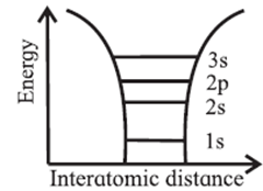
In Fig. horizontal lines indicate the allowed energy levels of an isolated sodium atom while the curved lines indicate the potential energy of an electron near the nucleus due to the Coulomb force.
Formation of energy bands in a solid :
- An isolated atom is characterized by discrete and well-defined allowed energy levels. For example, the electron configuration of an isolated sodium atom is 1s2 2s2 2p6 3s1.
- When two sodium atoms are brought sufficiently close together, by the Pauli exclusion principle, the individual electrons can no longer be in the same quantum state. Then, each original energy level is split into two different energy levels.
- A crystalline solid consists of a periodically repeating arrangement of a large number, say N, of the atoms, ions or molecules of the solid.
- At the small interatomic distance a (a ~0.37 nm in sodium, for example), these atoms interact strongly due to which each of the discrete energy level of an individual atom split to N such levels in the crystal.
- For each shell (1s 2s 2p, etc.), the energies of these N levels differ so slightly (of the order of 10-19 eV) that the distribution of these energy levels is very nearly continuous and said to constitute an energy band.
- Thus, bands of allowed energies are formed which the electrons can occupy, separated by bands of forbidden energies.

- Energy bands differ in the number of electrons they hold. In sodium, each energy level in the 1s and 2s energy bands holds up to two electrons with opposite spins, so each of these bands have a maximum occupancy of 2N electrons.
- The 2p energy band has a maximum occupancy of 6N electrons. But the 3s energy band is half filled with only N electrons.
- For a linear array of sodium atoms, the curved lines in Fig. show the periodic Coulomb potential, which drops as —1/r at each lattice point, where r is the distance from the nucleus.
- Inner shell electrons are closer to the nucleus of the parent atom. However, with the lowered Coulomb potential between the atoms, as shown in above Fig. the valence electrons constitute a single system of electrons common to the entire crystal with overlapping of their outermost electronic orbits.
- In sodium, the half-filled 3s energy band is the valence band. The next higher energy band is called the conduction band.
Energy bands in sodium :The following figure shows the energy levels and bands in solid sodium. The electronic configuration of sodium is 1s2 2s2 2p6 3s1. If there are N atoms in a solid piece of sodium, its 3s valence band will contain N energy levels which can hold 2N electrons. Thus, the 3s band in sodium is only half filled by electrons.

When sufficient energy is provided to an electron in the valence shell, that is, 3s electron, it can pick up additional energy while remaining in the original band. The additional energy is in the form of kinetic energy (KE), and the drift of the electron constitute an electric current.
Important Terms :
- Conduction band : At or near absolute zero of temperature, the empty energy band above the valence band is called the conduction band. It is formed of conduction levels.
- Valence band : The highest occupied energy band in a solid, formed by valence energy levels, is called the valence band.
- Band gap : The difference between the energies of the bottom of the conduction band and the top of the valence band is important for electrical conduction in a solid and is called the energy gap or the band gap.

- Fermi level : In a solid, the energy at which one half of the quantum states are occupied by the particles such as electrons is called the Fermi level.
- Valence level : The highest occupied energy level in an atom is called the valence level.
- Conduction level : The immediate next higher level which the electrons from the valence band can occupy on providing sufficient energy is called the conduction level.
Classification of solids on the basis of the band theory of solids :
Solids tend to be classified as conductors, semiconductors, and insulators based on their electrical characteristics. The variation in electrical conductivities may be explained using band theory.
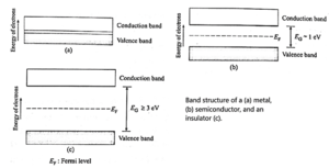
- In a metal, the conduction band and the valence band overlap. As a result, both the number of electrons and the variety of energy levels in which they may flow are very huge. An electron can shift into a higher energy state, absorb energy from the field, and participate in electrical conduction when there is an external electric field present.
- The forbidden energy gap (EG) between the conduction band and valence band of a semiconductor is fairly small, of the order of 1 eV. At room temperature, some of the electrons near the top of the valence band acquire thermal energy greater than EG and more into the conduction band. When an electric field is applied across the material, these electrons can thus take part in the electrical conduction.
- An insulator has a very wide energy gap between the valence band and the conduction band, EG ≥ 3 eV. Thermal energies at room temperature or even energies due to a strong electrical field are much less than 3 eV to transfer any electron from the valence band to the conduction band.
Intrinsic Semiconductor:
Intrinsic semiconductor: A pure, perfect semiconductor with an ideal crystal structure is called an intrinsic semiconductor. For example, Silicon and germanium
Structure of silicon :
The atomic number of silicon is 14. Its electronic configuration is 1s2 2s2 2p6 3s2 3P2 and valency is 4. In a crystal, each atom of Si forms four covalent bonds with its neighbouring atoms. One Si atom is surrounded by four Si atoms at the corners of a regular tetrahedron shown in Fig.

Hole : The absence of an electron in the valence band (or an empty electron energy level in the valence band) of a semiconductor is called a hole.
- There are two different types of charge carriers in a semiconductor. One is the electron and the other is the hole or absence of electron.
- Under the influence of an external electric field, a hole behaves like a positive charge carrier, equal in magnitude to the electronic charge.
Formation of holes in an intrinsic semiconductor :
- In a semiconductor, the band gap is close to 1 eV. Near absolute zero, all valence electrons are firmly attached to their corresponding atoms, completing the covalent bands. The valence band is fully occupied while the conduction band is totally empty. Hence, the material behaves as a perfect insulator.
- At room temperature, thermal energy breaks a few covalent bonds and some valence electron, bridge the forbidden energy gap and move into the conduction band leaving behind empty energy states, holes, in the valence band. A hole can be considered as an effective positive charge equal to that of the electron.

Behaviour of an intrinsic (pure) semiconductor close to the absolute zero of temperature and at room temperature :
Close to the absolute zero of temperature :
- The valence band of a semiconductor, like pure germanium and silicon, is fully occupied while the conduction band is totally empty.
- Hence, the material behaves as a perfect insulator.
- The two bands are separated by an energy gap of the order of 1 eV.
At room temperature :
- A limited number of valence electrons acquire thermal energy greater than the energy gap.
- These electrons bridge the energy gap and move into the conduction band, leaving behind empty energy states, holes, in the valence band.
- The free electrons in the conduction band and the holes in the valence band serve as charge carriers under the influence of an external electric field. This leads to limited conductivity and, hence, pure germanium and silicon are semiconductors at room temperature.
- The number of conduction electrons per unit volume (about 1017 per m3 and the conductivity (between 103 S/m and 10-3 S/m) of a semiconductor are much less than those of a conductor.
Importance of energy gap in a semiconductor :
- A semiconductor, like Si or Ge, has a 1 eV energy gap(EG) between its valence and conduction bands, making it a perfect insulator. The valence band is fully occupied near 0K, while the conduction band is empty.
- At room temperature, only a few valence electrons gain thermal energy above Eg, the conduction band, leaving empty energy. These electrons travel into the valence band, where they form holes. In the presence of an external electric field, free electrons in the conduction band and holes in the valence band act as charge carriers, resulting in restricted electrical conductivity. The substance is no longer an insulator.
Why holes are not present in a conductor :
Explanation :
- The energy band diagram for a metal can be partially full or overlapping, with a large number of electrons and empty energy states.
- When an electric field is applied, an electron must move into a higher energy state to absorb energy.
- Valence electrons have a continuous range of unfilled energy states, allowing them to absorb even small energy increments and be available for conduction. This makes metals a good conductor of electricity, as they have a large number of conduction electrons per unit volume and conductivity, about 1028 per m3 and greater than 104 S/m, respectively.
- Thus, when a hole is created, it gets quickly filled with an electron and hence holes are not present in a conductor.
Factors on which the electrical conductivity of a pure semiconductor depend at a given temperature :
- the width of the band gap between the valence band and the conduction band.
- the charge carrier concentration.
Conduction process in a semiconductor :
- Electrical conduction in a semiconductor takes place by two types of charge carriers, namely electrons and holes.
- The transport of any one or both carriers results in the electrical conduction.
- When an electric field is applied to a semiconductor by connecting a battery across it, the free electrons being negatively charged move towards the positive terminal of the battery.
- At the same time, the holes being positive charge carriers move towards the negative terminal of the battery and constitute the hole current (Fig.).
- Electrons and holes move in opposite directions and contribute to the conventional current from the positive terminal to the negative terminal of the battery in the external

Motion of electrons and holes in a semiconductor :
- A hole is a vacant electron energy level found in a semiconductor's valence band, which is otherwise filled.
- A neighboring atom's valance electron that has been released from its covalent bond by thermal energy resides in the empty energy state that results from this.
- This causes the neighboring atom to have a hole in its original place. As a result, a hole really travels in the opposite direction from an electron.
- An electron from a nearby covalent bond then fills this new hole, and the hole continues to migrate in the opposite direction of the electron. As a result, as electrons move in one direction, holes move in the opposite direction.
Electron current : An electric field on a semiconductor or metal causes free electrons in the conduction band to move in a direction opposite to the applied field, forming an electron current.
Hole current : When an electric field is applied to a semiconductor, the holes in the valence band move in the direction of the applied field due to a motion of negatively charged electrons in the opposite direction. This motion of holes constitutes a hole current.
Extrinsic semiconductors:
Extrinsic semiconductor : When a limited and controlled amount of certain impurity atoms, known as dopants, is introduced into an intrinsic semiconductor to drastically alter its electrical properties, the resultant material is known as an extrinsic or doped semiconductor.
Doping :
- Doping is the introduction of specific impurity atoms, called dopant, to an intrinsic semiconductor to alter its electrical properties.
- Doping significantly increases the concentration of charge carriers. Depending upon the valency of the dopant, an extrinsic semiconductor may be a p-type (with holes as majority charge carriers) or an n-type (with electrons as majority charge carriers).
- Dopant atoms are substitutional impurities, and their size should be comparable to the atom they replace.
Need of doping an intrinsic semiconductor :
Intrinsic semiconductors have low electrical conductivity at room temperature. However, adding dopant impurities increases the number of free electrons or holes, thereby increasing their electrical conductivity. The type and amount of dopant control this conductivity, enabling the fabrication of various electronic devices.
Acceptor and donor impurities :
(i) Acceptor impurities : Acceptor impurities are trivalent impurity atoms that accept valence electrons from neighboring atoms, resulting in holes in the valence band.
- When trivalent impurity atoms are used to dope a tetravalent semiconductor, one electron deficiency per impurity atom produces a large concentration of holes in the valence band, which add to the intrinsic hole concentration. Conduction in such an extrinsic semiconductor is largely due to holes. Therefore, in this case, holes are said to be majority charge carriers.
- The small number of electrons in the conduction band form the minority charge carriers.
- Examples of trivalent impurity : Boron (B), gallium (Ga), aluminium (Al).
(ii) Donor impurities : Donor impurities are pentavalent impurity atoms that donate excess electrons, making them available for conduction in tetravalent semiconductor doping.
- When pentavalent impurity atoms are used to dope a tetravalent semiconductor, each impurity atom donates its excess electron which becomes available for conduction.
- An extrinsic semiconductor formed by doping a tetravalent semiconductor with a pentavalent impurity has electrons as majority charge carriers and holes as minority charge carriers.
- Examples of pentavalent impurity : Phosphorus (P), arsenic (As), antimony (Sb).
Therefore extrinsic semiconductors are of two types :
- An n-type semiconductor, in which the electrons are the majority charge carriers and the holes are the minority charge carriers.
- A p-type semiconductor, in which the holes are the majority charge carriers and the electrons are the minority charge carriers.
The valency of the dopant will depend on the type of extrinsic semiconductor desired -p- or n-type.
(i) n-type semiconductor :
- An n-type semiconductor is formed when a crystal of silicon or germanium is doped with a pentavalent impurity such as phosphorus, arsenic or antimony.
- Four of the five electrons of an impurity atom form covalent bonds with four nearest neighbor atoms.
- The fifth electron of the pentavalent atom is weakly bound. For example, the ionization energy of antimony is 0.039 eV in Si, much less than the band gap energy of EG = 1.12 eV in Si. So, donor level ED is added 0.039 eV below the conduction band edge EC, from which the weakly bound electron is readily raised to the conduction band by thermal energy. Thus, the donor impurity atoms add electrons to the conduction band without creating holes in the valence band.

- Free electrons contributed by impurity atoms greatly increase the small concentration of free electrons already present in the material due to thermal energy.
- The electron concentration in the conduction band (ne) greatly exceeds that of thermal holes in the valence band (nh) : ne >> n Conduction in such an extrinsic semiconductor is largely electronic.
- Such an extrinsic semiconductor is, therefore, called a negative charge carrier type or an n-type semiconductor.
Features of an n-type semiconductor :
- In an n-type semiconductor, the material is doped with a pentavalent impurity. In this case electrical conduction takes place with electrons as majority charge carriers.
- The pentavalent impurity loses an electron and becomes positively charged.
- The appreciably and the number of holes remains number of free electrons increases the same as obtained from the source. For an n-type semiconductor, ne >> nh. Thus, free electrons are majority carriers and holes are minority carriers.
- These negatively charged free electrons and positively charged holes are available for conduction on applying the potential difference across the semiconductor.
| Know This :
One cm3 specimen of a metal or semiconductor has of the order of 1022 atoms. In a metal, every atom donates at least one free electron for conduction, thus 1 cm3 of metal contains of the order of 1022 free electrons, whereas 1 cm3 of pure germanium at 20 °C contains about 4.2×10²² atoms, but only 2.5×10¹³ free electrons and 2.5×10¹³ holes. Addition of 0.001% of arsenic (an impurity) donates 1017 extra free electrons in the same volume and the electrical conductivity is increased by a factor of 10,000. |
(ii) p-type semiconductor :

- A p-type semiconductor is formed when a crystal of silicon or germanium is doped with a trivalent impurity such as boron, gallium or aluminium.
- The three valence electrons of an impurity atom form covalent bonds with three of the four nearest-neighbour host atoms.
- One of the four bonds remains incomplete and needs an additional electron.
- A valence electron of a neighbouring atom may become free and complete the bond, leaving behind a hole. For example, the ionization energy of boron is 0.045 eV in Si, much less than the band gap energy of EG= 1.12 eV in Si.
- So, acceptor level EA is added 0.045 eV above the valence band edge Ev which can readily accept a valence electron at room temperature.
- Thus, the acceptor impurity atoms create holes in the valence band without adding electrons to the conduction band.
- Such impurity holes greatly increase the small concentration of holes already present in the material due to thermal energy.
- The hole concentration in the valence band (nh) greatly exceeds that of thermal electrons in the conduction band (ne) : nh >> ne. Conduction in such an extrinsic semiconductor is largely due to holes. Such an extrinsic semiconductor is, therefore, called a positive charge carrier type or p-type semiconductor.
Features of p-type semiconductor:
These are materials doped with trivalent impurity atoms (acceptors). Electrical conduction in these materials is due to holes as majority charge carriers.
- The acceptor atoms acquire electron and become negatively charged-ions.
- Number of holes is very large compared to the number of free electrons. (nh >> ne). Holes are majority charge carriers.
- When energy is supplied externally, positively charged holes (majority charge carriers) and negatively charged free electrons (minority charge carriers) are available for conduction.
Charge neutrality of extrinsic semiconductors:
- In an n-type semiconductor, a pentavalent atom adds a free electron, making the donor atom positively charged. This electron is electrically neutral, as each atom is neutral. The excess electrons in an n-type semiconductor are needed to complete covalent bonds in a semiconductor crystal. These extra free electrons increase the conductivity of the semiconductor.
- In contrast, in a p-type semiconductor, some energy levels contain holes or electron absence, and when an electron fills this level, the host atom becomes positively charged and the dopant atom becomes negatively charged, ensuring the semiconductor is electrically neutral.
- Thus, n-type as well as p-type semiconductors are electrically neutral.
Remember :
- The net charge in an extrinsic semiconductor (n-type or p-type) is zero
Relation between ne, nh and ni :
In thermal equilibrium for a semiconductor, ne.nh = ni2
Here,
ni = the number of intrinsically generated electrons per unit volume of the semiconductor,
ne = the number of conduction electrons per unit volume of the semiconductor and
nh = the number of holes per unit volume of the conductor.
ne and nh are thus the electron and hole concentrations respectively.
We reply to valid query.