Notes-Part-1
|
Topics to be Learn : Part-1
|
Introduction
The AC mains voltage is rectified by using junction diodes to obtain a DC voltage.
- pn-junction diode : A two terminal semiconductor device consisting of a pn-junction is called a pn-junction diode.
- Depletion region : The neighbourhood of the junction between a p-type layer and an n-type layer within a single semiconducting crystal is depleted of free (or mobile) charge carriers. This is called the depletion region or depletion layer.
- Barrier potential : The electric potential difference across the pn-junction is called the potential barrier or barrier potential.
- When the diode is forward biased, it behaves as a closed switch and current flows in the diode circuit. When the diode is reverse biased, it behaves as an open switch and no current flows in the diode circuit.
- Open-Close switching action of a diode allows it to be used as a rectifier.
Forward-biased state :
- The diode is said to be forward biased when the positive terminal of a cell is connected to the p side of the junction and the negative terminal to the n side.
- When forward biased, the depletion region narrows, lowering the potential barrier. As a result, the bulk of charge carriers from each region cross into the other region.
- When forward biased, the diode conducts in this manner; the total current across the junction is referred to as the forward current and is caused by both electron and hole currents. A forward-biased junction diode has an extremely low resistance and functions as a closed switch due to the narrowing of the depletion region.
Reverse-biased state :
- When a cell or battery's positive terminal is attached to the junction's n side and its negative terminal to its p side, a pn-junction diode is said to be reverse biased.
- The depletion region grows and the potential barrier rises when reverse-biased.
- The reverse-biased junction diode exhibits a high resistance, and the majority charge carrier concentration in each region drops in comparison to the equilibrium values.
- Diffusion current no longer flows over the junction. As a result, the diode is said to be in a quiescent or non-conducting condition when reverse biased, acting as an open switch (almost).
p-n Junction Diode as a Rectifier :
- The process of converting an alternating voltage (or current) to a direct voltage (or current) is called rectification.
- A circuit or device that is used to convert an alternating voltage (or current) to a direct voltage (or current) is called a rectifier.
- A rectifier produces a unidirectional but pulsating voltage from an alternating voltage.
- When an alternating voltage is applied across a pn-junction diode, the diode is forward-biased and reverse-biased during alternate half cycles.
- During the half cycle when the diode is forward-biased, it conducts. Therefore, there is a current through it from the p-region to the n-region.
- During the next half cycle, it is reverse-biased and does not conduct. Therefore, current passes only in one direction through the circuit. This way, a pn-junction diode acts as a rectifier.
Q. Why we need rectification/rectifiers ?
Alternating voltage is now used to generate, transmit, and distribute electrical energy because it is easier and more cost-effective to do so than to do so with direct current.
Alternating voltage is frequently used instead of direct voltage for the practical reason that alternating voltage may easily be altered in magnitude using a transformer.
However, most electrical and electronic systems need a dc voltage to work. Since the transmitted voltage is very high and alternating, we need to reduce the ac line voltage and then convert it to a relatively constant dc output voltage.
The power-line voltage is sequentially stepped down at the distribution substations. At the consumer end, the ac voltage is rectified using junction diodes to dc voltage.
Diagram and explanation of how to convert ac line voltage to dc output voltage:
A dc power supply is a part of consumer electronics that converts ac source voltage into a relatively steady dc voltage. A functional block diagram of the circuits inside a power supply is shown in the figure below.
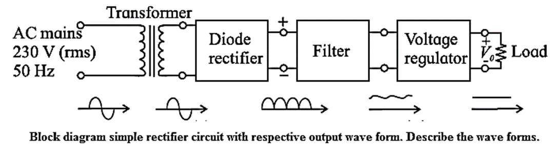
- The secondary voltage of the transformer that typically steps down the ac supply voltage is then transformed into a pulsing dc by a diode rectifier.
- This rectifier output can be viewed as having two distinct components according to the superposition theorem: a dc voltage (the average value) and an ac voltage (the fluctuating part).
- The filter circuit eliminates the pulsed dc. Nearly all of the ac component is blocked, and nearly all of the dc component is transferred to the load resistor.
- The filtered output for a rectified full-wave DC is depicted in the above figure. The little ac load voltage known as ripple is the only variation from a perfect dc voltage. The ripple is reduced using a filter circuit with good design.
- By doing this, we are able to produce a dc voltage that is practically ideal and nearly consistent, similar to the voltage coming from a battery.
- A power supply's regulation refers to its capacity to maintain a constant output under conditions of fluctuating input or shifting loads.
- The output voltage tends to decrease as power supplies are loaded and reach a lower value. Particularly in low-voltage power supply, an integrated circuit (IC) voltage regulator is now linked between a filter and a load resistor.
- In addition to reducing ripple, this device maintains constant output voltage despite changes in load and ac input voltage.
Half Wave Rectifier :
A device or a circuit which rectifies only one-half of each cycle of an alternating voltage is called a half-wave rectifier.
Electric circuit : The alternating voltage to be rectified is applied across the primary coil (PQ ) of a transformer. The secondary coil (AB) of the transformer is connected in series with the junction diode and a load resistance RL, as shown in below fig.

The alternating voltage across the secondary coil is the ac input voltage Vin. The dc voltage across the load resistance is called the output voltage Vout.
Working :
- Due to the alternating voltage Vin, the p-region of the diode becomes alternatively positive and negative with respect to the n-region.
- During the half-cycle when the p—region is positive, the diode is forward biased and conducts.
- A current IL passes through the load resistance RL in the direction shown.
- During the next half cycle, when the p-region is negative, the diode is reverse biased and the forward current drops to zero.
- Thus, the diode conducts only during one-half of the input cycle and thus acts as a half-wave rectifier.
- The intermittent output voltage Vout has a fixed polarity but changes periodically with time between zero and a maximum value. IL is unidirectional.
- Below figure shows the input and output voltage waveforms.

- The pulsating dc output voltage of a half-wave rectifier has the same frequency as the input.
Full Wave Rectifier:
A device or a circuit which rectifies both halves of each cycle of an alternating voltage is called a full-wave rectifier.
Electric circuit : The alternating voltage to be rectified is applied across the primary coil (PQ) of a transformer with a centre-tapped secondary coil (AB). The terminals A and B of the secondary are connected to the two p-regions of two junction diodes D1 and D2, respectively. The centre-tap C is connected to the ground. The load resistance RL is connected across the common n-regions and the ground.

Working: During one half cycle of the input, terminal A of the secondary is positive while B is negative with respect to the ground (the centre-tap C). During this half cycle, diode D1 is forward biased and conducts, while diode D2 is reverse biased and does not conduct. The direction of current IL through RL is in the sense shown.
During the next half cycle of the input voltage, B becomes positive while A is negative with respect to C. Diode D2 now conducts sending a current IL through RL in the same sense as before. D1 now does not conduct.
Thus, the current through RL flows in the same direction, i.e., it is unidirectional, for both halves or the full-wave of the input. This is called full-wave rectification.

The output voltage has a fixed polarity but varies periodically with time between zero and a maximum value. Above figure shows the input and output voltage waveforms. The pulsating dc output voltage of a full-wave rectifier has twice frequency of the input.
Advantages of a full wave rectifier :
- Rectification takes place in both the cycles of the AC input.
- Efficiency of a full wave rectifier is higher than that of a half wave rectifier.
- The ripple in a full wave rectifier is less than that in a half wave rectifier.
Remember :
|
Ripple Factor:
- The output of a rectifier consists of a small fraction of an AC component along with DC called the ripple.
- This ripple is undesirable and is responsible for the fluctuations in the rectifier output.
- The effectiveness of a rectifier depends upon the magnitude of the ripple component in its output. A smaller ripple means that the rectifier is more effective.
Figure shows the ripple in the output of a rectifier.

The ratio of root mean square (rms) value of the AC component to the value of the DC component in the rectifier output is known as the ripple factor, i.e.,
Ripple Factor = \(\frac{\text{rms value of ac component}}{\text{average value of dc component}}\)
Percentage ripple = ripple factor x 100%
Filter circuits:
- The output of a rectifier is in the form of pulses. The output is unidirectional but the output does not have a steady value. It keeps fluctuating due to the ripple component present in it.
- The circuit used in a dc power supply to remove the ripple is called a filter.
- A filter circuit can produce a very smooth waveform that approximates the waveform produced by a battery.
- The most common technique used for filtering is a capacitor connected across the output of a rectifier.
A capacitor filter:
Consider a simple capacitive filter added to a full-wave rectifier circuit, Fig. (a). A capacitor is a charge storage device that it can deliver later to a load.

- In the first quarter cycle, the capacitor charges as the rectifier output peaks. Later, as the rectifier output drops off during the second quarter cycle, the capacitor discharges and delivers the load current.
- The voltage across the capacitor, and the load, decreases up to a point B when the next voltage peak recharges the capacitor again.
- To be effective, a filter capacitor should be only slightly discharged between peaks. This will mean a small voltage change across the load and, thus, small ripple.
- As shown in Fig. (b), the capacitor supplies all the load current from A to B; from B to C, the rectifier supplies the current to the load and the capacitor.
- The discharging time constant of a filter capacitor has to be long as compared to the time between the voltage peaks.
- For the same capacitor used with a half-wave rectifier, the capacitor will have twice the time to discharge, and the ripple will be greater.
- Thus, full-wave rectifiers are used when a low ripple factor is desired.
Unregulated power supply : A dc power supply whose output changes when a load is connected across it is called unregulated power supply.
Regulated power supply : A dc power supply whose preset output voltage remains constant irrespective of variations in the line voltage or load current is called a regulated power supply.
Voltage regulation : Voltage regulation is an important factor of a power supply.
- Regulation is its ability to hold the dc output steady under conditions of changing ac input or changing load.
- The output voltage under no-load condition (no current drawn from the supply) tends to drop to a lower value when load current is drawn from the supply (under load).
- The amount the dc voltage changes between the no-load and full-load conditions is described by a factor called voltage regulation.
Voltage regulation = \(\frac{no-load\,\,voltage-full\,\,load\,\,voltage}{full\,\,load\,\,voltage}\)
Special Purpose Junction Diodes:
Junction Break Down:
When a sufficiently large reverse voltage is applied to a pn-junction, there is an abrupt strong increase in the reverse current and its rectifying properties are lost. This is known as junction break-down. The absolute value VB of the voltage at which the phenomenon occurs is called breakdown voltage.
The breakdown process is not inherently destructive and is reversible.
Two important breakdown mechanisms are the Zener breakdown (due to tunneling effect) and avalanche breakdown (due to avalanche multiplication).
Zener Breakdown :
In a reverse-biased pn-junction, the depletion region is wider and the potential barrier is higher over equilibrium values. The electric field in the depletion region is from the n- to the p-region.
When a sufficiently large reverse voltage is applied to a pn-junction, the junction breaks down and conducts a very large current. Of the two important breakdown mechanisms, Zener breakdown takes place in heavily doped diodes.
Usually, the energy that an electron can gain from even a strong field is very small. However, the depletion region is very narrow in a heavily doped diode. Because of this, the electric field across the depletion region is intense enough to break the covalent bonds between neighbouring silicon atoms and pull electrons out of their orbits. This results in conduction electrons and holes. In the energy band diagram representation, this corresponds to the transition of an electron from the valence band to the conduction band and become available for conduction.
The current increases with increase in applied voltage, but without further increase in voltage across the diode. This process, in which an electron of energy less than the barrier height penetrates through the energy band gap, is called tunneling (a quantum mechanical effect).
The creation of electrons in the conduction band and holes in the valence band by tunneling effect in a reverse-biased pn-junction diode is called the Zener effect.
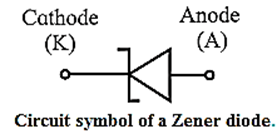
Zener Diode:
- A Zener diode works on the principle of junction breakdown.
- A Zener diode is a heavily doped pn-junction diode operated in its breakdown region.
- Zener break-down occurs when the breakdown voltage is less than about 6 V while avalanche breakdown occurs in lightly doped diodes and for breakdown voltage greater than 6 V.
- However, the Zener effect was discovered before the avalanche effect, so all diodes used in the breakdown region came to be known as Zener diodes.
I-V characteristics of a Zener diode :
The forward bias region of a Zener diode is identical to that of a regular diode. There is forward current only after the barrier potential of the pn-junction is overcome. Beyond this threshold or cut in voltage, there is an exponential upward swing
The typical forward voltage at room temperature with a current of around 1 mA is around 0.6 V.

In the reverse bias condition the Zener diode is an open circuit and only a small reverse saturation current flows as shown with change of scale. At the reverse breakdown voltage there is an abrupt rapid increase in the current-the knee is very sharp, followed by an almost vertical increase in current.
The voltage across the Zener diode in the break-down region is very nearly constant with only a small increase in voltage with increasing current.
There is a minimum Zener current, IZ (min), that places the operating point in the desired break-down region. At some high current level, IZM, the power dissipation of the diode becomes excessive beyond which the diode can be damaged.
Zener diode as a voltage regulator
Principle : In the breakdown region of a Zener diode, for widely changing Zener current, the voltage across the Zener diode remains almost constant.
Electric circuit : The circuit for regulating or stabilizing the voltage across a load resistance RL against change in load current and supply voltage is shown in Fig.
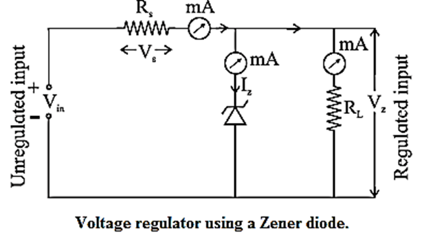
The Zener diode is connected parallel to load RL such that the current through the Zener diode is from the n to p region. The series resistance RS limits the current through the diode below the maximum rated value.
From the circuit, I = IZ + IL and V = IRS + VZ = (IZ + IL)RS + VZ
Working of a Zener Regulator :
When the input unregulated dc voltage V across the Zener diode is greater than the Zener voltage VZ in magnitude, the diode works in the Zener breakdown region. The voltage across the diode and load RL is then VZ. The corresponding current in the diode is IZ.
As the load current (I) or supply voltage (V) changes, the diode current (IZ) adjusts itself at constant VZ. The excess voltage V—VZ appears across the series resistance RS.
For constant supply voltage, the supply current I and the voltage drop across Rs remain constant. If the diode is within its regulating range, an increase in load current is accompanied by a decrease in IZ at constant VZ.
Since the voltage across RL remains constant at VZ, the Zener diode acts as a voltage stabilizer or voltage regulator.
Use of a resistor in series with a Zener diode :
The I-V characteristics in the breakdown region of a Zener diode is almost vertical. That is, the current IZ can rapidly increase at constant VZ.
To prevent damage due to excessive heating, the Zener current should not exceed the rated maximum current, IZM.
Hence, a current-limiting resistor RS is connected in series with the diode.
IZ and the power dissipated in the Zener diode will be large for IL = 0 (no-load condition) or when IL is less than the rated maximum (when RS is small and RL is large). The current-limiting resistor Rs is so chosen that the Zener current does not exceed the rated maximum reverse current, IZM when there is no load or when the load is very high.
The rated maximum power of a Zener diode is
PZM = IZM = VZ
At no-load condition, the current through RS is I = IZM and the voltage drop across it is V− VZ,
where V is the unregulated source voltage. The diode current will be maximum when V is maximum at Vmax and I = IZM. Then, the minimum value of the series resistance should be
RS min = (Vmax − VZ )/IZM
Applications of Zener Diode: The Zener diode is used when a constant voltage is required.
It has a number of applications such as:
- Voltage regulator,
- Fixed reference voltage provider in transistor biasing circuits,
- Peak clipper or limiter in a wave shaping circuit,
- Protector against meter damage from accidental fluctuations, etc.
Know This :
|
Photo Diode :
- A photodiode is a reverse-biased pn-junction special-purpose diode that produces charge carriers in response to photons and high-energy particles and transmits a photocurrent proportionate to the intensity of the incident radiation in the external circuit.
- The term photo-diode usually means a sensor that accurately detects changes in light level. Hence, it is sometimes called a photodetector or photosensor which operates as a photoelectric converter.

Construction :
- An n-type silicon substrate and a metal electrode back contact constitute a photodiode.
- The n-type substrate is covered with a thin p-type layer by diffusing an appropriate acceptor dopant.

- The area of the p-layer defines the photodiode active area. An ohmic contact pad is deposited on the active area.
- The rest of the active area is left open with a protective antireflective coating of silicon nitride to minimize the loss of photons.
- The non-active area is covered with an insulating opaque SiO2 coating.
- Depending on the required spectral sensitivity, i.e., the operating wavelength range, typical photo-diode materials are silicon, germanium, indium gallium arsenide phosphide (InGaAsP) and indium gallium arsenide (InGaAs), of which silicon is the cheapest while the last two are expensive.
Working :
- The band gap energy of silicon is EG = 1.12 eV at room temperature. Thus, photons or particles with energies greater than or equal to 1.12 eV, which corresponds to λ <= 110 nm, can transfer electrons from the valence band into the conduction band.

- A photodiode is operated in the reverse bias mode which results in a wider depletion region.
- When operated in the dark (zero illumination), there is a reverse saturation current due solely to the thermally generated minority charge carriers. This is called the dark current. Depending on the minority carrier concentrations, the dark current in an Si photodiode may range from 5 pA to 10 nA.
- When exposed to radiation of energy hv 2 EC (in the range near-UV to near-IR), electron-hole pairs are created in the depletion region.
- The electric field in the depletion layer accelerates these photo-generated electrons and holes towards the n side and p side, respectively, constituting a photocurrent I in the external circuit from the p side to the n side.
- Due to the photogeneration, more charge carriers are available for conduction and the reverse current is increased. The photocurrent is directly proportional to the intensity of the incident light. It is independent of the reverse bias voltage.
I-V characteristics of a photodiode :
When a Si photodiode is operated in the dark (zero illumination), the current versus voltage characteristics observed are similar to the curve of a rectifier diode as shown by curve (1) in Fig. This dark current in Si photodiodes range from 5 pA to 10 nA.
When light is incident on the photodiode, the curve shifts to (2) and increasing the incident illuminance (light level) shifts this characteristic curve still further to (3) in parallel.
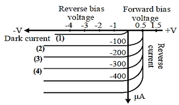
The magnitude of the reverse voltage has nearly no influence on the photocurrent and only a weak influence on on the dark current. The normal reverse currents are in tens to hundreds of microampere range.
The almost equal spacing between the curves for the same increment in luminous flux reveals that the reverse current and luminous flux are almost linearly related. The photocurrent of the Si photodiode is extremely linear with respect to the illuminance. Since the total reverse current is the sum of the photocurrent and the dark current, the sensitivity of a photodiode is increased by minimizing the dark current.
Saturation current of the photodiode :
As you can see from the below curve, reverse current increases initially with increase in the intensity of illumination. It reaches a constant value after certain voltage is reached. This constant value is called the saturation current of the photodiode.
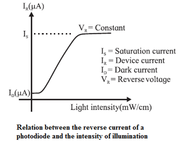
Dark current : The current associated with a photodiode with an applied reverse bias during operation in the dark (zero illumination) due to background radiation and thermally excited minority saturation current. It is of the order of picoamperes to nanoamperes. Larger active areas or increase in temperature and reverse bias result in higher dark current.
Dark resistance : The ratio of maximum withstandable reverse voltage to the dark current of a photodiode is called dark resistance of that diode.
Dark resistance, Rd = \(\frac{maximum\,\,reverse\,\,voltage}{dark\,\,current}\)
Advantages of photodiode
- Quick response when exposed to light.
- Linear response. The reverse current is linearly proportional to intensity of incident light.
- High speed of operations.
- Light weight and compact size.
- Wide spectral response. For example, photodiodes made from Si respond to radiation of wavelengths from 190 nm (UV) to 1100 nm (IR).
- Relatively low cost.
Disadvantages of photodiode
- Its properties are temperature dependent, similar to many other semiconductor devices.
- Low reverse current for low illumination levels.
Applications of photodiode
A photodiode has many applications in a number of fields ranging from domestic applications to industrial applications due to its linear response.
The basic concept used in almost all these devices/applications is that a photodiode conducts whenever light strikes it and it stops conducting the moment light stops.
Some applications of a photodiode are:
- Counters and switches.
- Burglar alarm systems.
- Detection of visible and invisible radiations.
- Circuits in which fast switching and high speed operations are required.
- Fiber optic communication systems.
- Optocouplers, used to provide an electric isolation between two electronic circuits.
- Photo sensors/detectors, for accurate measurement of light intensity.
- Safety electronics like fire and smoke detectors
Solar Cell or Photovoltaic Cell:
Two major types of devices converting solar energy in usable form are,
- Photo thermal devices which convert the solar energy into heat energy. Mostly used for providing hot water.
- Photo voltaic devices which convert solar energy into electrical energy using solar cells.
Solar Cell : A solar cell is an unbiased pn-junction that converts the energy of sunlight directly into electricity with a high conversion efficiency.
Principle : A solar cell works on the photovoltaic effect in which an emf is produced between the two layers of a pn-junction as a result of irradiation.
Structure of a Solar Cell:
- A p-type semiconductor substrate is backed by a metal electrode back contact in a simple pn-junction solar cell.
- By doping with an appropriate donor impurity, a thin n-layer (less than 2.5 pm for silicon) is created over the p-type substrate.
- Metal finger electrodes are formed on top of the n-layer, leaving enough space between the fingers for sunlight to reach the n-layer and, ultimately, the underlying pn-junction.

Working : When exposed to sunlight, the absorption of incident radiation (in the range near-UV to infrared) creates electron-hole pairs in and near the depletion layer.
- Consider light of frequency v incident on the pn-junction such that the incident photon energy hv is greater than the band gap energy EC of the semiconductor.
- The photons excite electrons from the valence band to the conduction band, leaving vacancies or holes in the valence band, thus generating electron—hole pairs.

- The photogenerated electrons and holes move towards the n side and p side, respectively. If no external load is connected, these photogenerated charges get collected at the two sides of the junction and give rise to a forward photo-voltage.
- In a closed-circuit, a current I passes through the external load as long as the solar cell is exposed to sunlight.
- A solar cell module consists of several solar cells connected in series for a higher voltage output.
- For outdoor use with higher power output, these modules are connected in different series and parallel combinations to form a solar cell array.
V-I Characteristic of solar Cell or Photovoltaic cell:
Below fig. shows the I-V characteristic of solar cell when illuminated. This is drawn in the fourth quadrant because a solar cell supplies current to the load.

- The output characteristic, V-I curve, of a solar cell exposed to sunlight is plotted by varying the load resistance (RL) from zero to infinity and measuring the corresponding current and voltage.
- The short-circuit condition occurs when RL = 0 so that V = 0. The current in this case is referred to as the short-circuit current ISC. The open-circuit condition occurs when RL = ∞. The net current in this case is zero and the voltage produced is called as the open-circuit voltage VOC.
- Increasing the light-sensing area or light intensity per single solar cell produces a proportionate increase in ISC. VOC is independent of these parameters.
- The operating point of a solar cell module is the point (VP, IP) on the I —V curve which delivers maximum power to the load. For this, VP / IP must be equal to RL.
Criteria for selection of material for solar cell:
- Its band gap should be between 1.0 eV to 1.8 eV.
- It should have high optical absorption (conversion of light into electrical energy).
- It should have good electrical conductivity.
- Material should be easily available.
- The cost of the material must be low
Materials used for solar cells :
Most materials used for fabrication of solar cells are have a band gap of about 1.5 eV. These include: Si, GaAs, CdTe, CuInSe.
Some of the common materials for solar cells are
- Silicon (Si), EG = 1.12 eV— currently the most popular material but has low absorption coefficient and high temperature dependence.
- Gallium arsenide (GaAs), EG = 1.42 eV—by far the most widely used, especially for high end applications like satellites. Its absorption coefficient is about ten times better than silicon and doesn't have the same temperature dependence.
- Copper-indium diselenide (CIS), EG=1.01 eV—has the highest optical absorption, but gallium is introduced in the lattice to raise the band gap energy closer to the solar ideal. This resulted in the popular copper-indium—gallium diselenide (CuIn-GaSe2 or CIGS) material for photovoltaic cell. By variation of Ga fraction, a band gap of around 1.48 eV has been achieved.
- Cadmium telluride (CdTe), EG=1.44 eV—made from the II—VI group elements.
Use of Solar cell:
Solar cells used in domestic and space applications/
- A solar cell array, which consists of a collection of solar cells, is used during the day to power electrical equipment as well as to recharge batteries, which can then be utilised at night.
- Solar cell arrays supply electrical power to satellite equipment as well as isolated locations on Earth where electric power cables do not exist.
- Solar power generation systems on a large scale that are linked to the commercial power grid.
- Independent power supply systems for radar detectors, monitoring systems, radio relay stations, roadlights and roadsigns.
- Indoor uses include consumer products like, calculators, clocks, digital thermometers, etc. (They use very low levels of power and work under low-brightness long-wavelength light from incandescent lamps, etc.)
Know This :
|
Light Emitting Diode / LED:
The Light Emitting Diode or LED as it is more commonly called is a diode which emits light when large forward current passes through it.

- It is formed from compound semiconductor materials such as gallium arsenide (Ga/ls) in which light emission can take place from direct radiative recombination of excess electron-hole pairs.
- A photon is emitted when an electron in the conduction band recombines with a hole in the valence band.
- In infrared emitting LEDs, the encapsulating plastic lens may be impregnated or coated with phosphorus. Then, phosphorescence of the phosphorus gives off visible light.
Structure of LED :
- A light-emitting diode is a forward-biased pn-junction diode formed from compound semiconductor materials. The top metal contact to the n-layer (say) is provided with a window for the emitted light to escape.
- The diode chip is encapsulated in a transparent plastic lens. The cathode and anode leads from the metal contacts to the n-and p-layers, respectively, are provided for external connections, Fig. (b).
- The negative electrode (cathode) is identified by a notch or flat spot on the plastic body, or the cathode lead is shorter than the anode.

Working of a LED:
- Figure (a) schematically shows the emission of light when electron-hole pair combines. When the diode is forward biased, electrons from the semiconductor's conduction band recombine with holes from the valence band releasing sufficient energy to produce photons which emit a monochromatic (single colour) light
- The resulting photon has an energy approximately equal to the bandgap of the active layer material. Modifying the bandgap of the active layer creates photons of different energies.
- In the energy band diagram this recombination is equivalent to a transition of the electron from a higher energy state in the conduction band to a lower energy state in the valence band. The energy difference is eniitted as a photon of energy hv.
- The amount of light output is directly proportional to the forward current. Thus, higher the forward current, higher is the light output.
Factors on which the intensity and colour of the light emitted by an LED depend :
The intensity of the emitted light is directly propertional to the recombination rate and hence to the diode forward current.
The colour of the light emitted by an LED depends on the compound semiconductor material used and its composition (and doping levels) as given below :
LEDs are made with elements such as gallium, phosphorus and arsenic. By varying the proportions of these elements in the semiconducting materials, it is possible to produce light of different wavelengths.
- LED made using aluminium gallium arsenide (AlGaAs), it emits infrared radiations.
- LED made using gallium arsenic phosphide (GaAsP) produces either red or yellow light,
- LED made by using aluminium gallium phosphide (AlGaP) emits red or green light
- LED made by using zinc selenide (ZnSe) produce blue light.
I-V Characteristics Light Emitting Diodes:
Below figure shows the I-V characteristic of LED. It is similar to the forward characteristic of an ordinary diode.
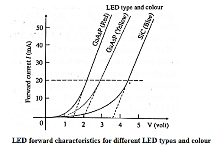
- The diode starts conducting only after the forward-bias voltage overcomes the barrier potential. Thereafter the current increases exponentially beyond the knee region.
- The threshold voltage is about 1.2 V for a standard red LED to about 3.6 V for a blue LED.
- However, these values depend on the manufacturer because of the different dopant concentrations used for the different wavelength ranges.
- The intensity of the emitted light is directly propotional to the forward current.
- An LED is operated with a typical forward current of 20 mA — about 5 mA for a simple LED indicator to about 30 mA where a high intensity of light is needed.
- The LED forward current must be limited to a specified safe value using a series resistance.
- The peak inverse voltage (PIV) or breakdown voltage of an LED is low, typically 5 V.
Know This :
|
Advantages of LED:
LED is a solid state light source.
- Energy efficient: More light output for lesser electrical power. LEDs are now capable of producing 135 lumens/watt
- Long Lifetime: 50,000 hours or more if properly manufactured.
- Rugged: LEDs are also called Solid State Lights (SSL) as they are made of solid material with no filament or tube or bulb to break.
- Fast switching : Almost no warm up period. LEDs start emitting light in nanoseconds.
- Excellent colour rendering: Colours produced by LED do not fade out making them perfect for displays and retail applications.
- Environment friendly : LEDs do not contain mercury or other hazardous substances.
- Controllable: Brightness and colour of light emitted by LEDs can be controlled
Disadvantages of an LED :
- Blue light hazard : There is a photobiological concern that bright blue LEDs and cool-white LEDs are capable of exceeding safe limits.
- Light quality : Most cool-white LEDs have spectral output significantly different from the Sun or an incandescent bulb—peak output being at 460 nm rather than peak retinal sensitivity of 550 nm. This can cause the colour of objects to be perceived differently under cool-white LED illumination than sunlight or incandescent bulbs.
- Temperature dependence : An LED luminaire can overheat in high ambient temperatures and effective cooling methods using heat sinks are essential for high-power LEDs. This is especially important for automotive, medical and military applications where the light unit must operate over a large range of temperatures and yet have a low failure rate.
- High initial cost : LEDs are currently more expensive price per lumen in initial capital cost, than most conventional lighting technologies.
- Voltage sensitivity : LEDs must be operated with the voltage above the threshold and the current below the rated maximum. This requires current-limiting resistors or current-regulated power supplies.
- Blue light pollution : Cool-white LEDs emit proportionally more blue light than conventional out-door light sources such as high-pressure sodium lamps. Due to Rayleigh scattering, these LEDs can cause more light pollution than other light sources.
Applications of LEDs :
- On electrical equipment, an LED is commonly used as an on/off indicator lamp.
- LEDs are used in self-illuminating seven-segment alphanumeric displays such as calculators, digital clocks and metres, signage, and so on.
- LEDs are currently widely utilised in traffic signals, handheld torches, LED TV sets, residential and decorative lights, and other indication lamps in light motor vehicles and two-wheelers due to their low power consumption.
- The virtually monochromatic light emitted by an LED is also coherent under certain conditions. These diode lasers have found use in optical fibre communications, CD players, CDROM drives, laser printers, bar code scanners, laser pointers, and other devices.
| Know This :
LED lamps, bulbs, street lighting are becoming very popular these days because of the very high efficiency of LEDs in terms of light output per unit input power(in milli Watts), as compared to the incandescent bulbs. So for general purpose lightings, white light is preferred. Commercially available white LEDs are normally manufactured by using the technique of wavelength conversion. It is a process which partly or completely converts the radiation of a LED into white light. There are many ways of wavelength conversion. One of these methods uses blue LED and yellow phosphor. In this method of wavelength conversion, a LED which emits blue colour is used to excite a yellow colour phosphor. This results in the emission of yellow and blue light and this mixture of blue and yellow light gives the appearance of white light. This method is the least expensive method for producing white light. |
We reply to valid query.