Notes-Part-2
Topics to be Learn : Part-2
|
Bipolar Junction Transistor (BJT):
A junction transistor is a semiconductor device having two junctions and three terminals.
- The current in a transistor is carried by both the electrons and the holes. Hence, it is called a bipolar junction transistor.
- A junction transistor consists of two back-to-back pn-junctions forming a sandwich structure in which a thin layer of n—type or p—type semiconductor is sandwiched between two layers of opposite type semiconductor.
- The three terminals of a transistor connected to its three layers are known as the emitter (E), base (B) and collector (C).
- One pn-junction is between the emitter and the base while the other pn-junction is between the collector and the base.
There are two types of junction transistors: (i) pnp transistor (ii) npn transistor.
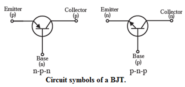
The arrow on the emitter shows the direction of current when the base-emitter junction is forward-biased. If the arrow points in (Points iN), it indicates the transistor is a pnp. On the other hand, if the arrow points out, the transistor is an npn (Not Pointing iN ).
Formation of junction transistor and Structure of the two types of BJTs :
- A bipolar junction transistor has three separately doped regions and two pn-junctions.
- A pnp transistor is formed by starting with a p-type substrate. An n-type region is grown by thermally diffusing donor impurities into this substrate. A very heavily doped p+ region is then diffused into the n—type region. The heavily doped p + -region is called the emitter, symbol E in Fig.
- The narrow central n-region, with lightly doped concentration, is called the base (symbol B). The width of the base is small compared with the minority carrier diffusion length.
- The moderately doped p-region is called the collector (symbol C). The doping concentration in each region is assumed to be uniform.
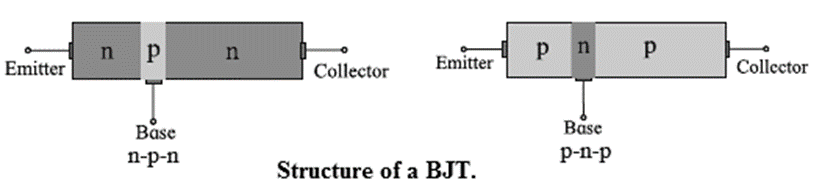
- The npn transistor is the complementary structure to the pnp transistor : A narrow p region grown into an n type substrate, by thermally diffusing acceptor impurities, forms the base. The heavily doped n + region diffused into the base forms the emitter.
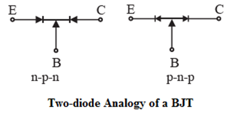
Two-diode analogy : A transistor can be thought to be two junction diodes connected back to back. This two-diode analogy is shown in below fig.
Emitter: It is a thick heavily doped layer. This supplies a large number of majority carriers for the current flow through the transistor
Base: It is the thin, lightly doped central layer.
Collector: It is on the other side of the base. It is thick and moderately doped layer. Its area is larger than that of the emitter and the base. This layer collects a major portion of the majority carriers supplied by the emitter. The collector also helps dissipation of any small amount of heat generated.
Depletion region: The depletion regions are formed at the emitter-base junction and the base-collector junction.
Current: Current indicates in circuit is as : The emitter current IE, the base current IB and the collector current IC
Resistance: The emitter-base junction has low resistance while the base-collector junction has a high resistance.
Working of a p-n-p transistor:
For normal operation of a junction transistor, the emitter-base junction is always forward biased and the collector-base junction is always reverse biased.
Figure shows the biasing of the junctions for an npn transistor connected as an amplifier with the common-base configuration, that is, the base lead is common to the input and output circuits.
- The emitter-base junction is forward biased by the battery VBB while the collector-base junction is reverse biased by the battery VCC. VBB should be greater than the emitter-base barrier potential (the threshold voltage). The arrows of the various currents indicate the direction of current under normal operating conditions (also called the active mode).
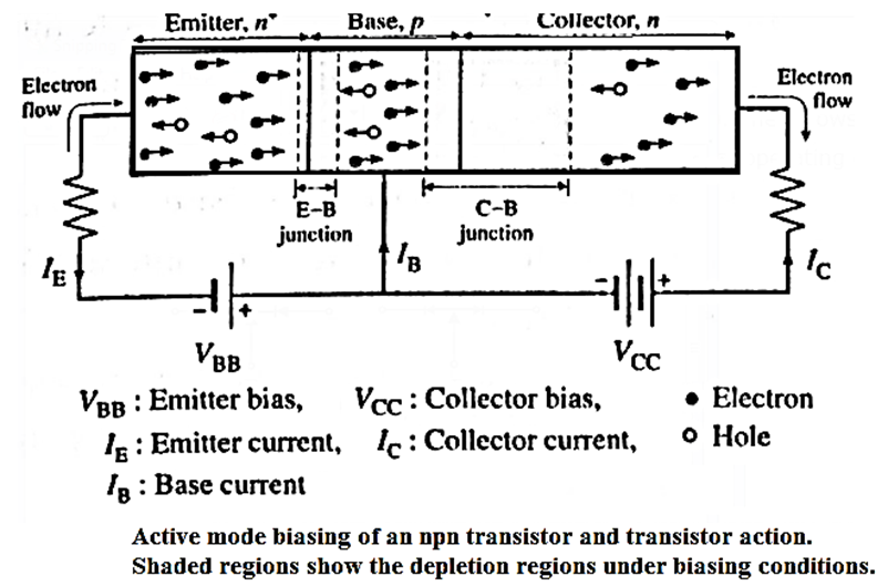
- Because the emitter-base junction is forward biased, electrons from the n+ emitter are injected into the base, while holes from the p-type base are injected into the emitter. These two current components make up the total emitter current IE under ideal-diode conditions.
- The emitter is an n-type area that has been highly doped. As a result, the current flowing between emitter E and base B is virtually exclusively electron current flowing from E into B over the forward-biased emitter junction.
- The p—type base is narrow and has a very low hole density. As a result, nearly all of the injected electrons (more than 95%) diffuse directly through the base to the collector junction without recombining with holes. Because the collector junction is reverse biased, electrons that reach there are quickly swept by the high electric field into the n-type collector region, where they form the collector current IC.
- In practice, about 1% to 5% of the holes from the emitter recombine with holes in the base layer and cause a small current IB in the base lead.
- Therefore, IE = IB + IC ≈ IC.
- Therefore, carriers injected from a nearby emitter junction can result in a large current flow in a reverse-biased collector junction. This is the transistor action, and it can be realized only when the two junctions are physically close enough to interact as described.
- If a pnp transistor is used, the battery connections must be reversed to give the correct bias. The conduction process is similar but takes place instead by migration of holes from emitter to collector. A few of these holes recombine with electrons in the base.
| Remember :
The lightly doped, thin base region sandwiched between the heavily doped emitter region and the intermediate doped collector region plays a crucial role in the transistor action. |
Transistor configuration:
The possible configurations of transistor in a circuit are,
- Common Emitter, CE
- Common Base, CB and
- Common Collector, CC.
Common Emitter configuration : The emitter of the transistor is common to both the input and the output, Fig. (a).
Common Base configuration : The base of the transistor is common to both the input and the output, Fig. (b).
Common Collector configuration : The collector of the transistor is common to both the input and the output, Fig. (c).
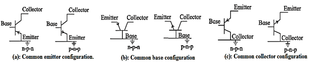
(1) CE : Produces the highest current and power gain of all the three bipolar transistor configurations- the reason why it is the most commonly used configuration for transistor based amplifiers. The emitter is grounded and the input signal applied between the base and emitter. The input impedance is small due to the forward biasing of the EB-junction. The output taken from between the collector and emitter, as well as the output impedance, are large due to the reverse biased CB-junction. However, its voltage gain is much lower.
(2) CB : The base terminal is grounded, the input signal is applied between the base and emitter terminals while the output signal is taken from between the base and collector terminals. Though its high frequency response is good for single stage amplifier circuits, it is not very common due to its low current gain characteristics and low input impedance.
(3) CC : Very useful for impedance matching applications because of the very large ratio of input impedance to output impedance. The collector is grounded and the input signal is directly given to the
Relation between current gains α and β for a transistor :
The dc common-base current ratio or current gain (αdc) is defined as the ratio of the collector current to emitter current.
αdc = IC/IE
The dc common-emitter current ratio or current gain (βdc) is defined as the ratio of the collector current to base current.
βdc = IC/IB
Since the emitter current IE =IB + IC,
IE/IC = IB/IC + 1
∴ \(\frac{1}{α_{dc}}=\frac{1}{β_{dc}}+1\)
Therefore, the common—base current gain in terms of the common-emitter current gain is
αdc = \(\frac{β_{dc}}{1+β_{dc}}\)
and the common-emitter current gain in terms of the common-base current gain is
βdc = \(\frac{α_{dc}}{1-α_{dc}}\)
Since the electrical relationship between these three currents IB, IC and IE is determined by the physical construction of the transistor itself, any small change in the base current (IB), will result in a much larger change in the collector current (IC). Thus, a small change in current flowing in the base will control the current in the emitter-collector circuit.
The Common Emitter (CE) characteristic:
A typical circuit used to study the common emitter (CE) characteristic is shown in the Fig.
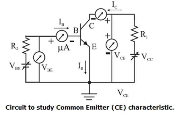
The Input characteristics: This is a set of curves of base current IB against base to emitter voltage VBE for different constant collector to emitter voltages VCE, Fig.
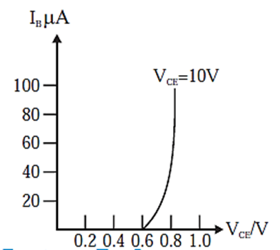
Keeping collector voltage VCE constant, base voltage is gradually increased from zero. Initially, IB is zero till VBE is less than the threshold voltage for the forward-biased base-emitter junction. For VBE greater than the threshold voltage, IB increases steeply.
For a constant collector voltage VCE, the dynamic input resistance (ri) is defined as the ratio of the differential change in the base-to-emitter voltage (ΔVBE) to the corresponding change in the base current (ΔIB ).
ri = \((\frac{ΔV_{BE}}{ΔI_B})_{V_{CE}=constant}\)
Output or collector characteristics : This is a set of curves of collector current IC against collector—to-emitter voltage VCE for different constant base currents IB, Fig.
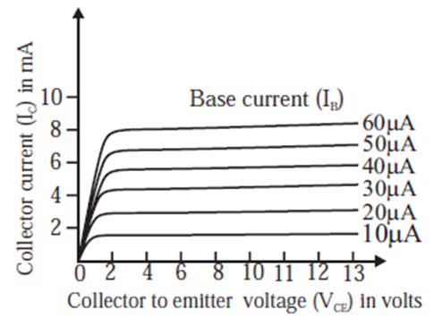
(i) For VBE less than the threshold voltage for the junction, IB = 0 and IC =0, i.e., there is no current through the transistor. Both the junctions are reverse biased and the transistor acts like an open switch. Then the transistor is said to be switched
Fully-OFF or in the cut-off region or OFF-mode.
(ii) The base current is set to a suitable value by varying the base—to-emitter voltage VBE to a value greater than the threshold voltage. Then, the collector-to-emitter voltage VCE is varied and the variation of IC is plotted against VCE. For very small values of VCE, ideally zero, IC is maximum, equal to VCC / RL. Both the junctions are forward biased and the transistor acts like a closed switch. The transistor is said to be switched Fully-ON, or in the saturation region or ON-mode.
(iii) But for values of VCE above about the threshold voltage, IC is constant and VCE has relatively little effect on it. In this region, called as the active region, IC is determined almost entirely by IB. In this region, the common-emitter current gain β is large.
For a constant base current IB, the dynamic output resistance ( rO) is defined as the ratio of the differential change in the collector-to-emitter voltage (ΔVCE) to the corresponding change in the collector current (ΔIC )
rO = \((\frac{ΔV_{CE}}{ΔI_C})_{I_B=constant}\)
Transistor as an Amplifier:
Amplifier is a device which is used for increasing the amplitude of the alternating signal (voltage, current or power).
Principle : The collector current can be controlled by a small change in the base current.
Electric circuit : Consider the use of a npn transistor as an amplifier in the widely used common-emitter (CE) configuration in which the emitter is common to the input and output circuits, Fig.

The emitter-base junction is forward biased by the battery VBB while the collector—base junction is reverse biased by the battery VCC.
The voltage V, to be amplified, called the signal voltage, is applied between the base and the emitter.
Working :.The collector characteristics shows that in the active region, the collector current IC is determined almost entirely by the base current IB, and collector potential VC has relatively little effect on it.
Let us discuss the working of the amplifier when the input signal Vi is not applied.
Consider the output loop. We have, from the Kirchhoff’s law,
VCC − ICRL−VCE = 0 …..(1)
and VBB − IBRB − VBE = 0 ……(2)
The applied signal voltage causes small changes ΔVBE in the emitter-base p.d. thereby producing variations ΔIB in the base current.
ΔVBE = riΔIB ….(3)
where ri is the dynamic input resistance.
VBB + Vi = IBRB + VBE + ΔIB(RB + ri)
Vi = ΔIB(RB + ri)= riΔIB because RB is small.
The variations in ΔIB cause proportionately larger variations ΔIC in the collector current because ΔIC = βac ΔIB, where the ac common-emitter current gain (βac) is always greater than 50. For normal operating voltages, βac is almost the same as βdc.
From Eq. (1), since VCC is constant,
ΔVCC = ΔICRL + ΔVCE = 0
The time-varying collector current produces a time-varying output voltage VO across the load resistance RL.
Vo = ΔVCE = − ΔICRL = − βac ΔIBRL
Thus, VO > Vi, so that the circuit produces a voltage gain. The amplifier's voltage gain (Av) is defined as the ratio of the output voltage to the input voltage. '
Av = VO/Vi = \(-\frac{β_{ac}R_L}{r_i}\)
The minus sign indicates that the output voltage is 180° out of phase with the input voltage.
We know that there is also a current gain βac in the common emitter configuration. We can therefore write the power gain Ap as,
Ap = βac Av
We have ignored the negative sign for the voltage gain to write the magnitude. A transistor can be used to gain power because βac > 1
| Know This :
Transistor as a switch : A switch is a device that is used to open (or break) and close a circuit. A bipolar transistor, either npn or pnp, may be used as a switch. When used as a switch, a bipolar transistor is operated in the cut-off region (open switch) and saturation region (closed switch). Advantages of a transistor as a switch :
Uses :
|
Logic Gates :
Analog signal :
An analogue signal is a voltage or current that varies continuously. An analogue electrical circuit receives an analogue signal as input and produces a signal that varies continuously in response to the input signal.
Digital signal :
- A digital signal consists of a sequence of electrical pulses whose waveform is approximately regular, with the potential switching alternately between two values.
- The lower value of the potential is labelled as LOW or 0 and the higher value as HIGH or 1.
- With just two bits of information, 1 or 0 (HIGH or LOW), digital circuits use binary system.
- A sequence of 1s and 0s is encoded to represent numerals, letters of the alphabet, punctuation marks and instructions.
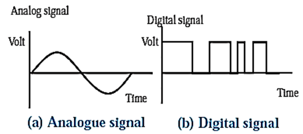
Digital circuit : An electronic circuit that processes only digital signals is called a digital circuit. There are only two voltage states present at any point within a digital circuit. These voltage states are either high or low.
The branch of electronics which deals with digital circuits is called digital electronics.
Logic gate : A logic gate is a basic switching circuit used in digital circuits that determines when an input pulse can pass through to the output. It generates a single output from one or more inputs.
Explanation/Uses :
- Any digital computation method involves conducting a series of arithmetic operations on the problem's data.
- The type of the operation to be done at each stage in the calculation is dictated partly by the pre-specified programme and partly by the results of previous stages in the process.
- To perform logical processes, we need switches with many inputs, i.e., the outputs of these switches are determined in certain ways by the condition (binary state) of their inputs. These configurations are known as logic gates, and they are typically an expansion of a simple transistor switch.
A logic gate can be represented by its logic symbol, Boolean expression and the truth table.
Boolean expression : An equation expressing a logical compound statement in Boolean algebra is called a Boolean expression. A Boolean expression for a logic gate expresses the relation between input(s) and output of a logic gate.
Truth table : The table which shows the truth values of a Boolean expression for a logic gate for all possible combinations of its inputs is called the truth table of logic gate.
The truth table contains one row for each input combination. Since a logical variable can assume only two possible values, 0 and 1, there are 2N combinations of N inputs so that the table has 2 N rows.
Example : Rows in the truth table of a 3-input gate : Each of the 3 inputs can take 2 values (0 and 1). Hence, the number of rows in the truth table of a 3-input gate = 2 x 2 x 2 = 23 = 8.
Types of logic gates :
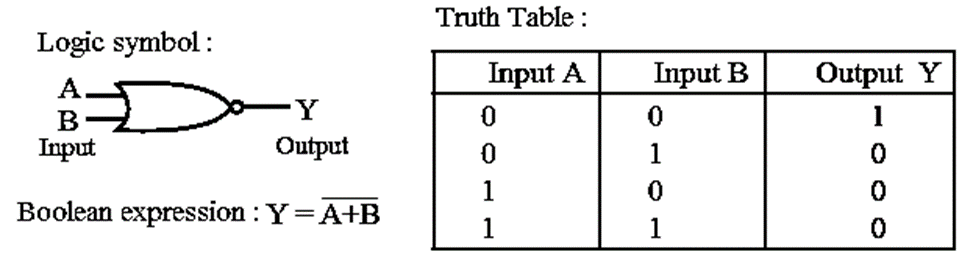
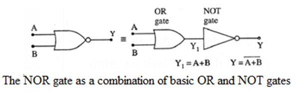
- The five common logic gates are the AND, OR, NOT, NAND and NOR gates.
- Of these the AND, OR and NOT gates which respectively perform the logical AND, logical OR and logical NOT operations are called the basic logic gates. These three gates form the basis for other types of logical gates.
- The NAND and NOR are called the universal logic gates because any gate can be implemented by the combination of NAND and NOR gates.
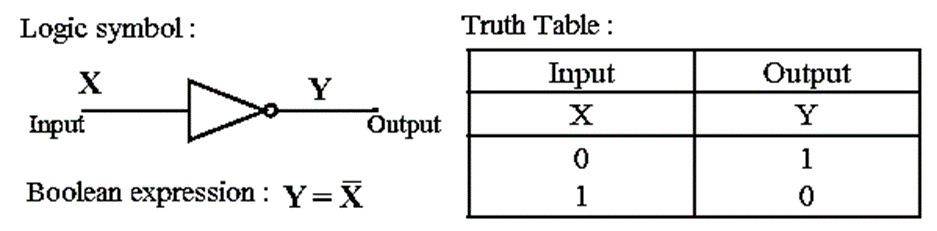
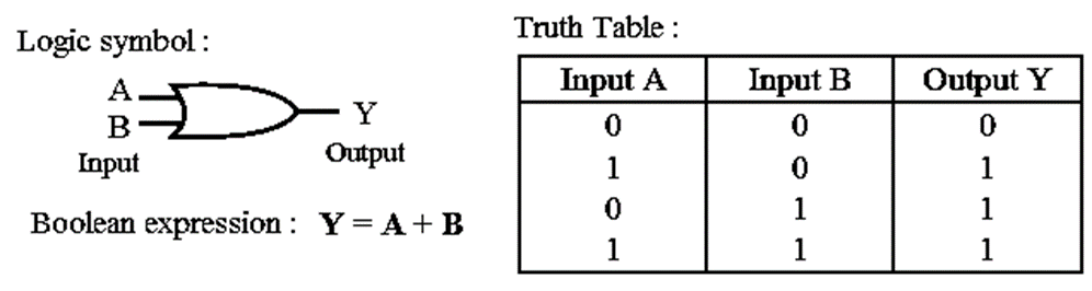
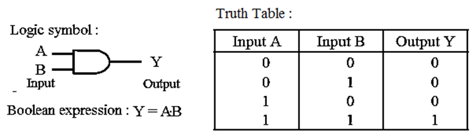
NOT gate or INVERTER : It is a circuit with one input whose output is HIGH if the input is LOW and vice versa. The NOT operation outputs an inverted version of the input. Hence, a NOT gate is also known as an INVERTER. The small invert bubble on the output side of the inverter logic symbol, Fig. and the over bar (—) in the Boolean expression represent the invert function. OR gate : It is a circuit with two or more inputs and one output in which the output signal is HIGH if any one or more of the inputs is HIGH. The OR operation represents a logical addition. Fig. shows the 2-input OR gate logic symbol, and the Boolean expression and the truth table for the OR function. AND gate : It is a circuit with two or more inputs and one output in which the output signal is HIGH if and only if all the inputs are HIGH simultaneously. The AND operation represents a logical multiplication. Figure shows the 2-input AND gate logic symbol and the Boolean expression and the truth table for the AND function. NAND gate : It is a circuit with two or more inputs and one output, whose output is HIGH if any one or more of the inputs is LOW; the output is LOW if all the inputs are HIGH. The NAND gate is a combination of an AND gate followed by a NOT gate so that the truth table of the NAND function is obtained by inverting the outputs of the AND gate. NOR gate : It is a circuit with two or more inputs and one output, in which the output is HIGH if and only if all the inputs are LOW. The NOR gate is realized by connecting the output of OR gate to the input of a NOT gate, so that thetruth table of the NOR function is obtained by inverting the outputs of the OR gate.

Exclusive OR/ X-OR Gate :
It is a circuit with only two inputs and one output in which the output signal is HIGH if and only if the inputs are different from each other.
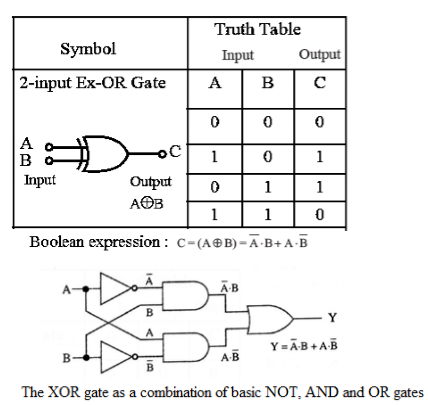
- The Exclusive-OR logic function is a very useful circuit that can be used in many different types of computational circuits.
- The ability of the Exclusive-OR gate to compare two logic levels and produce an output value dependent upon the input condition is very useful in computational logic circuits.
We reply to valid query.