Notes Part-2
Topics to be Learn : Part -2
|
p-n junction :
pn-junction : A surface within a single crystal of a semiconductor at which there is an abrupt change (nearly) in doping from acceptor to donor type is called a pn-junction.

- One method of fabricating a pn—junction is to introduce acceptor impurities from one end and donor impurities from the opposite end of an intrinsic semiconductor crystal. This brings about the change from a p-type to an n-type region in a very short length called the pn-junction.
- The thickness of the junction between p and n regions is of the order of 10-6 The impurity concentrations in the p-and n-sides, and thus the majority charge carrier densities, usually differ by a factor of 10 or 102 or even more.
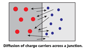
Diffusion: A pn-junction creates a significant variation in charge carrier concentrations, with electrons being majority carriers on the n-side and holes being majority carriers on the p-side. These carriers move from high concentration to low concentration regions, a process known as carrier diffusion, influenced by their density gradient.
Depletion region : The region of the junction between a p-type layer and an n-type layer within a single semiconducting crystal is depleted of free (or mobile) charge carriers. This is called the depletion region or depletion layer.
Formation of potential barrier in a pn-junction :
- The electron concentration in an n-type layer is much greater than that in a p-type layer. When a pn—junction is formed, this sharp density gradient causes some electrons from the n-layer to diffuse into the p-layer.
- These electrons combine with positive holes near the junction in the p-layer so that uncompensated negative charges of acceptor atoms are left uncovered.
- The diffusion of electrons leaves uncompensated positive charges of donor atoms near the junction in the n-layer.
- A similar reasoning also applies to holes, which diffuse from the p-layer into the n-layer.
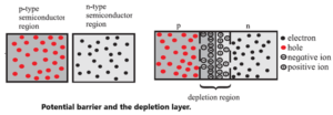
- Thus, the neighbourhood of the junction is depleted of free (or mobile) charge carriers, holes and electrons, and a depletion region is formed. The width of the depletion region in an unbiased pn-junction diode ranges from 0.5 μm to 1 μm, and depends on the dopant concentrations.
- Because of the positively charged donor ions on the n side of the depletion region and negatively charged acceptor ions on its p side, the n side of the depletion region is at a higher electric potential than the p side.
- This acts like a barrier and prevents further diffusion of free charge carriers across the junction, i.e., holes from the p-layer into the n-layer and electrons from the n-layer into the p-layer.
- The diffusion of charge carriers across the junction and resultant accumulation of positive and negative charges across the junction builds a potential difference across the junction.
- The electric potential difference (p.d.) across the pn—junction is called the potential barrier or barrier potential.
Know This :
- The potential barrier in an unbiased pn-junction diode maintains equilibrium between majority carrier holes in the p-region and minority carrier holes in the n-region, and also between majority carrier electrons in the n—region and minority carrier electrons in the p-region.
- The barrier potential is about 0.3 V for Ge junction diode and about 0.7 V for Si junction diode. However, this p.d. across the junction cannot be measured with a voltmeter.
- The width of the depletion region and the barrier potential depend on the bias voltage. They decrease with increasing forward bias and increase with increasing reverse bias.
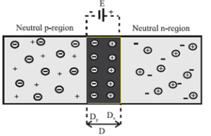
Electric field across a junction.
- The depiction region produced has a width D. The width of depletion region on the p-side is denoted by Dp and the width of depletion region on the n-side is Dn.
Potential barrier : The diffusion of charge carriers across a pn-junction, resulting in the accumulation of positive and negative charges, creates an electric potential difference, known as the potential barrier or barrier potential.
Biasing a p-n junction: Biasing a pn-junction means applying an external voltage across the junction. There are two ways an external voltage can be applied to a pn-junction, namely, forward bias and reverse bias.
- In forward bias, the positive terminal of a cell or battery is connected to the p-side of the junction and the negative terminal to the n-side.
- In reverse bias, the negative terminal of a cell or battery is connected to the p—side of the junction and the positive terminal to the n-side.
Effect of external voltage on the width of the depletion region in a pn-junction :
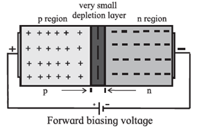
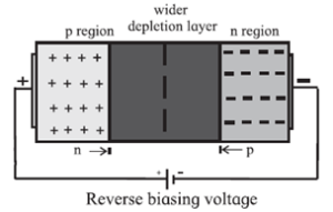
- In an unbiased pn-junction, the n-side has a higher electric potential than the p-side. An external voltage can be applied to control the width of the depletion region and barrier height.
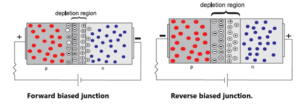
- Under forward bias[Fig.(a)], the applied voltage opposes the barrier, allowing electrons and holes to diffuse into the p-side and n-side. Some electrons and holes recombine with uncompensated donor and acceptor ions, reducing the width of the depletion region.
- Under reverse bias [Fig.(b)], the applied voltage increases the barrier potential. The reverse bias draws the majority carriers out of each region and the depletion region widens.
Need for biasing a pn-junction :
- In an open-circuit condition, a potential barrier prevents charge carriers from diffusing across a pn-junction, while biasing allows us to controls the depletion region width and barrier height.
- Under forward bias, majority charge carriers from each region can diffuse into the other over a lowered barrier. This is equivalent to conventional current in the material from the p- to the n-side, and the junction acts like a closed switch.
- Reverse bias increases the barrier height and stops the diffusion current. This near-zero current condition is equivalent to an open switch.
- Thus, biasing allows us to control the conducting state of a pm-junction.
Features of the depletion region:
- It is formed by diffusion of electrons from n-region to the p-region. This leaves positively charged ions in the n-region.
- The p-region accumulates electrons (negative charges) and the n-region accumulates the holes (positive charges).
- The accumulation of charges on either sides of the junction results in forming a potential barrier and prevents flow of charges across it.
- There are no charges in this region.
- The depletion region has higher potential on the n-side and lower potential on the p-side of the junction.
A p-n junction diode:
pn-junction diode : A two-terminal semi-conductor device consisting of a pn-junction is called a pn-junction diode. Figure indicates the circuit symbol for a pn—junction diode.
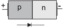
- The arrow shown here indicates the direction of conventional current. The p-side is called the anode while the n-side is called the cathode of the diode. There are two ways in which a diode can be connected across the battery, namely, forward bias and reverse bias.
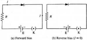
- Forward bias : The polarity of external voltage for which there is a large current through a pn-junction is called forward bias. Here, the positive terminal of a cell is connected to the p side of the junction and the negative terminal to the n side, Fig. (a).
- Reverse bias : The polarity of external voltage that restrains the current through a pn-junction to extremely small values is called reverse bias. In this case, the positive terminal of a cell is connected to the n side of the junction and the negative terminal to the p side, Fig. (b).
Working of a forward-biased pn-junction diode :
A forward biased pn-junction diode is a device where the positive terminal of a cell or battery is connected to the p side of the junction and the negative terminal to the n side.
- Under open-circuit conditions, the depletion region and potential barrier have equilibrium values. When forward biased, the depletion region narrows, lowering the potential barrier, causing charge carriers to cross into the other region.
- Electrons travel from the n side to the p side and to the positive terminal of the battery, while holes combine with electrons from the p side to the n side. This conducts the diode, resulting in a forward current due to both electron and hole currents.
- The conventional current direction is opposite to electron flow. This results in a low resistance and closed switch function.
Working of a reverse-biased pn-junction diode :
A pn-junction diode is reverse biased when the positive terminal of a cell or battery is connected to the n side of the junction, and the negative terminal to the p side.
- Under open-circuit conditions, the depletion region and potential barrier have equilibrium values.
- When reverse biased, the depletion region widens and the potential barrier increases, causing the majority charge carriers of each region to decrease against equilibrium values. This results in a high resistance, causing the diffusion current across the junction to become zero. The diode is in a quiescent or non-conducting state, acting as an open switch almost.
- However, a small current flows due to the motion of minority charge carriers, and the potential barrier aids the flow of these carriers, electrons in the p-region and holes in the n-region, to cross the junction in opposite directions, known as the reverse current.
Asymmetrical current flow in a pn-junction diode :
- The behavior of a diode in forward-biased and reverse biased modes is different due to the difference in barrier potential. In forward biased mode, the barrier potential is reduced, while in reverse biased mode, it is increased.
- Carriers can easily cross the junction in forward bias due to reduced barrier width and extra energy gain. This results in a large current through the diode, which is of the order of a few milliamperes (10-3 A) for a typical diode.
- Conversely, when connected in reverse bias, the width of the potential barrier increases, causing carriers to be pushed away from the junction, resulting in a small current. The width of the depletion layer decreases with forward voltage application and increases with reverse voltage application.
- When the bias voltage polarity is reversed, the width of the depletion layer changes, resulting in asymmetrical current flow through the diode.
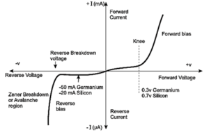
I-V characteristics for Ge and Si pn-junction diodes :
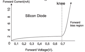
(i) I-V characteristic of a forward biased diode : Initially, the current is very low and then there is a sudden rise in the current. The point at which current rises sharply is shown as the ‘knee’ point on the I-V characteristic curve. The corresponding voltage is called the ‘knee voltage’. It is about 0.7 V for silicon and 0.3 V for germanium.
(ii) I-V characteristic of a reverse biased diode : Very high negative voltage results in a sharp change in the reverse-bias characteristics. At a certain characteristic negative voltage, called the peak inverse voltage (PIV) or breakdown voltage, the current in the reverse direction increases very rapidly. In general, a silicon diode has a higher PIV rating (~1000 V) than a germanium diode (~4OO V)
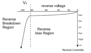
Avalanche breakdown :
When the reverse bias voltage on a diode is increased, it causes the p-n junction to overheat, leading to a sudden increase in current. This is due to the breaking of covalent bonds and the availability of more carriers for conduction. The diode, thus, no longer behaves like a diode. This effect is called the avalanche breakdown.
Zero Biased Junction Diode :
An open-circuited pn-junction diode across which no external voltage is applied is called an unbiased or zero-biased pn-junction diode.

- When diode terminals are shorted together, holes and electrons on the p-side and n-side (major charge carriers) cross the junction, overcoming the potential barrier and contributing to current. This diffusion, due to carrier concentration variation, results in the forward current.
- Similarly, some thermally generated holes in the n-side and electrons in the p-side (minority charge carriers), drift across the junction in the opposite direction and contribute to current. This current is known as the reverse current.
- Further diffusion of majority charge carriers across the junction is prevented by the potential barrier that builds up. However, minority charge carriers continue to drift across the junction aided by the potential barrier.
- A dynamic equilibrium occurs when majority charge carriers move in opposite directions, with a zero net diffusion current across the junction.
- However, a small leakage current, caused by minority charge carriers drifting across the depletion region, remains. As the temperature of the pn-junction rises, this equilibrium state changes, generating more minority charge carriers and increasing the leakage current.
Dynamic equilibrium : When the terminals of a pn-junction diode are shorted, the external p.d. across it is zero. Majority charge carriers in each region diffuse across the junction into the other region due to density gradient. An equilibrium reached as the number of electrons and holes moving in opposite directions are equal; ne = nh. This state is called dynamic equilibrium
Importance of the depletion region in a pn-junction diode :
The region of the junction between a p-type region and an n-type region within a single semiconducting crystal is depleted of free (or mobile) charge carriers. This is called the depletion region.
- The depletion region in a diode acts as a potential barrier, allowing diffusion of majority charge carriers across the junction.
- Under forward bias, the external voltage lowers the barrier height, allowing charge carriers to diffuse into the other region, causing the diode to conduct.
- Under reverse bias, the external voltage adds to the barrier potential, increasing the barrier height, stopping diffusion and causing the diode to enter a non-conducting state.
- This allows for control of the diode's conduction state like a switch, with forward bias acting like a closed switch and reverse bias acting like an open switch.
Static and dynamic resistance of a diode:
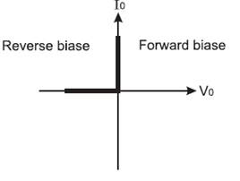
Ideal diode : An ideal diode offers zero resistance in forward biased mode and infinite resistance in reverse biased mode.
I-V characteristic of an ideal diode :
An ideal diode offers zero resistance in the forward biased mode and infinite resistance in the reverse biased mode. That means, an ideal diode is an electronic device in which conduction takes place instantly in the forward biased mode whereas no conduction takes place in the reverse biased mode.
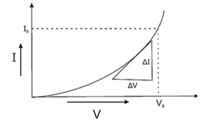
The I-V characteristics of a forward biased diode is used to define two of its resistances (i) the static (DC) resistance and (ii) the dynamic (AC) resistance.
(i) Static (DC) resistance : The resistance (R) offered by a diode when a current passes through it is called the static (dc) resistance of the diode. It is the ratio of the voltage across the diode to the current through it at a particular voltage.
rdc = \(\frac{V}{I}\)
(ii) Dynamic resistance of a diode : The dynamic (ac) resistance of a diode is the ratio of a small change in voltage (ΔV) across the diode to a small change in current (ΔI) through it.
rac = \(\frac{ΔV}{ΔI}\)
The dynamic resistance of a diode depends on the operating voltage. It is the reciprocal of the slope of the characteristics at that point.
Figure shows how the DC and the AC resistance of a diode are found out.
Example : Refer to the figure a shown below and find the resistance between point A and B when an ideal diode is (1) forward biased and (2) reverse biased.
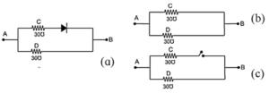
We know that for an ideal diode, the resistance is zero when forward biased and infinite when reverse biased.
(i) Figure (b) shows the circuit when the diode is forward biased. An ideal diode behaves as a conductor and the circuit is similar to two resistances in parallel.
RAB = (30 x 30)/(30+30) = 900/60 = 15 Ω
(ii) Figure (c) shows the circuit when the diode is reverse biased. It does not conduct and behaves as an open switch, path ACB. Therefore, RAB= 30 Ω, the
only resistance in the circuit along the path
Semiconductor devices:
Semiconductor devices find applications in variety of fields. They have have numerous advantages, but they also have some disadvantages.
Advantages:
- Electronic properties of semiconductors can be controlled to suit our requirement.
- They are smaller in size and light weight.
- They can operate at smaller voltages (of the order of few mV) and require less current (of the order of μA or mA), therefore, consume lesser power.
- Almost no heating effects occur, therefore these devices are thermally stable.
- Faster speed of operation due to smaller size.
- Fabrication of ICs is possible.
Disadvantages:
- They are sensitive to electrostatic charges.
- Not vary useful for controlling high power.
- They are sensitive to radiation.
- They are sensitive to fluctuations in temperature.
- They need controlled conditions for their manufacturing.
- Very few matreials are semiconductors.
Applications of semiconductors and p-n junction diode:
Solar cell : It is an unbiased pn-junction that converts the energy of sunlight directly into electricity with a high conversion efficiency. Solar cell arrays provide electrical power to equipment on a satellite, space probes and space stations as well as at remote places on the earth where electric power lines are absent.
Photodiode : It is a semiconductor device which converts light into an electric current.
Light Emitting Diode (LED) : It emits light when a current passes through it. Household LED lamps use similar technology. They consume less power, are smaller in size and have a longer life and are cost effective.
Solid state laser diode : If a special type of LED. It emits light of specific frequency. It is smaller in size and consumes less power.
Photo resistor ; It is a light-controlled variable resistor. It changes its resistance with the incident light.
Bipolar junction transistor: If is a three terminal electronic device that amplifies the flow of current. There are two junctions and three terminals in this device. A transistor can be a p-n-p or n-p-n type. The electric current is conducted by both free electrons and holes.
Many other types of transistors are designed and fabricated to suit specific requirements. They are used in almost all semiconductor devices.
Integrated Circuits (ICs) : A small device having hundreds of diodes and transistors performs the work of a large number of electronic circuits.
Thermistor:
A thermistor, for thermal resistor, is a temperature sensitive resistor of which resistance changes with a change in the temperature.
Types of thermistor and their uses :
The thermistors are of two types, having negative temperature coefficient (NTC) and positive temperature coefficient (PTC) of resistivity.
This indicates that, with the increasing temperature, the resistance of a NTC thermistor decreases. Whereas, the resistance of a PTC thermistor increases with the increasing temperature.
Uses :
(i) An NTC thermistor is used when a continuous change of resistance is required over a wide temperature range and is extensively used in applications such as
- temperature measurement
- temperature control in electrical circuits to prevent overheating
- temperature compensation in mobile communication equipment.
(ii) A PTC thermistor is used when a large change in resistance is required at a particular temperature or current and is used in applications such as
- a temperature sensor for protection of windings in motors and transformers
- a solid state fuse to protect circuits in the event of drawing too much current as in power supplies
- a liquid level sensor.
Electric and electronic devices :
- Electric devices : Electric devices convert electrical energy into various forms, such as fans, refrigerators, and geysers. Fans convert electrical energy into mechanical energy, while geysers convert it into heat energy. They use good conductors and have a common working range of milli amperes to amperes. Geysers consume moderate to high power, typically consuming 2.0 to 2.50 kW, and are moderate to large in size and costly.
- Electronic devices: Electronic devices, such as calculators, cell phones, smartwatches, and TV remotes, operate through controlled or sequential current changes via a cell. Semiconductors are used to fabricate these devices, which have a common working range of nano-ampere to μA, consume low energy, are compact, and cost-effective.
We reply to valid query.